 The ASIC business is getting more and more complicated. The ability to produce innovative die at a competitive price to solve increasingly complex problems just isn’t enough. The technology required to package that die is now front and center.
Here, at the junction of advanced design, process technology and state-of-the art packaging is where real innovation takes place. Perhaps nowhere does the importance of advanced packing technology, such as System in Package (SIP) and emerging 2.5D and 3D capabilities, become clearer than when you talk with the team at Global Unichip Corporation (GUC) who is emerging as a leader in the newly defined “Flexible ASIC” space.
Before jumping into a packaging discussion, it is important to define “Flexible ASIC.” At GUC, Flexible ASIC defines what they do: Provide access to foundry design environments to reduce design cycle time, provide custom IP and design methodologies to lower the barrier to entry, and integrate it all (design, foundry, assembly and test) for faster time–to–market. And that is where the emphasis on advanced packaging technology comes in.
The trend toward SiP (System in a Package) has been brought about because of the need to cram more and more flexibility into a smaller and smaller footprint to satisfy the demand of today’s 24/7 always connected electronic consumer. While this is clearly a great strategy, the challenges can be overwhelming. Here’s what the packaging experts have to say:
- First there is the issue of “known good die.” As more chips are integrated into a single package, the challenge of maintaining cost/effective yield grows almost exponentially.
- Then too, the design has to take in three dynamics … chip, package, and ultimately the board.
- Perhaps most critical are the thermal considerations created by stacking more die into a single package.
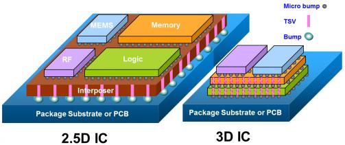
Two of the ways that GUC overcomes these challenges is through its Integrated Passive Device (IPD) technology, which is currently available, and a state-of-the art implementation of Through Silicon Via (TSV) Interposer Technology which will be available shortly.
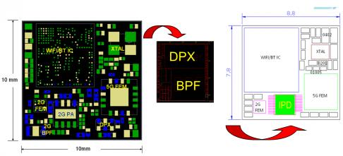
Using IPD technology, GUC successfully integrated some of the stand alone passive components. In the example below, GUC reduced passives by 50% and integrated both DPX and BPF. Total package size was reduced 31% from 10mm x 10mm to 8.8mm x 7.8mm and package thickness was reduced 17%.

One of the barriers to the more advanced 2.5D IC technology is cost, and while the process is not mature at this point sometimes the TSV on interposer is a significant cost consideration.
While solving that thorny conundrum, GUC has been working on the technology for five years, the company is also making significant progress toward pure 3D ICs. What makes 3D IC technology distinctive from its 2.5 D cousin is that pure 3D ICs have their TSV structures running direct to the chip area rather than to the interposer. GUC estimates that true 3D IC production is still a year or two off.
Despite the daunting challenges, GUC claims that providing an SiP approach accounts for around 25% of all new projects and 30% of its revenues. The company has shipped over 17 million SiP units targeting applications in consumer, wireless, network and computer applications. Furthermore, the company is finding a niche for what it calls “Ultra Large SiP” with package dimension over 50mm x 50mm.
Some of the more pessimistic pundits long ago declared the ASIC era dead, myself included. But clearly the complexity of providing more functionality in smaller and smaller footprints have given rise for the need of a new kind of ASIC company, a Flexible ASIC company, that can bring to the market services BEYOND design and manufacturing excellence.
That said, the real question is: What role will advanced packaging technology play in tomorrow’s innovation?


Captain America: Can Elon Musk Save America’s Chip Manufacturing Industry?