SpringSoft, soon to be part of Synopsys but officially still a separate company for now, just announced that Laker[SUP]3[/SUP], the third generation of their layout product family, is featured in TSMC’s 20nm Custom Reference Flow.
Laker 20nm advancements include new double patterning-aware design and voltage-dependent design rule checking (DRC) flows, enhanced flows for layout-dependent effect (LDE) and parasitic-aware layout, and advanced gradient density analysis capabilities. SpringSoft also collaborated with Mentor Graphics Corporation to qualify Laker-Calibre RealTime integration for signoff-quality, real-time DRC during custom layout.
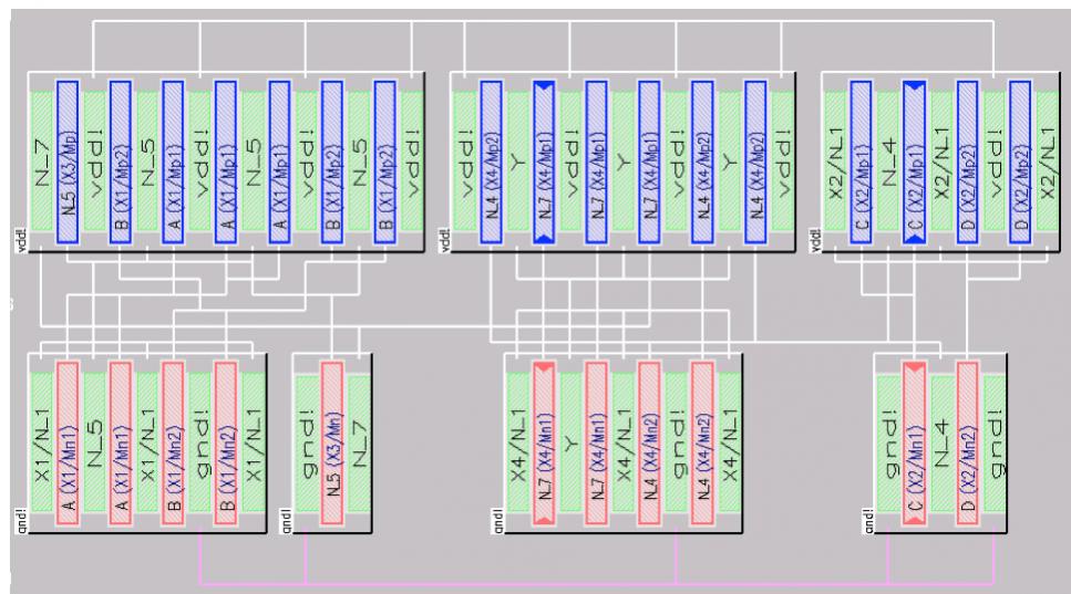
 Another feature of Laker is its symbolic design mode. Dave Reed told me that designers of 20nm standard cell libraries are finding that the design rules are so restrictive at 20nm that there are very limited options such as reordering transistors, all of which can be done quickly and easily in symbolic mode and then the layout automatically generated.
There are so many design rules at 20nm that it is next to impossible for a designer to comprehend them all and so the Laker-Calibre integration (both tools run off OpenAccess) giving signoff-quality DRC while doing interactive layout is pretty much essential. Designing the cells and then running a batch DRC from time to time is nowhere near fast enough. Just making sure the lower layers are all colorable for double-patterning, for example, is something where the designer wants instant feedback.
Laker’s first involvement with 20nm has been with a product called Laker Test Chip Designer. This is as early as you can get engaged since essentially you are working with the process development people. It is in use at many foundries. This is an interesting product since it doesn’t exactly have mass market appeal (when did you last design a process test chip with dozens of ring oscillators etc) but does get Laker involved very early so that they start to understand the issues and changes as soon as possible. And issues and changes there are at 20nm.
I would love to show you some 20nm layout so you can see just how different it is from what now seems like a do-what-you-like layout style for older process nodes. But everyone is so paranoid about what competitive manufacturers might deduce from seeing some that I’m not allowed to.


Siemens U2U 3D IC Design and Verification Panel