You are currently viewing SemiWiki as a guest which gives you limited access to the site. To view blog comments and experience other SemiWiki features you must be a registered member. Registration is fast, simple, and absolutely free so please,
join our community today!
I agree that this question sounds stupid: nobody is forcing me to buy an innovative product, or even a gadget, if I don’t want to pay a high price, I just don’t buy the product. But it seems that some people don’t really think that way. The story is related to Qualcomm sales in China, and recently announced partnership with SMIC…
The Partnership… Read More
Just to review: The brain inside the current Apple iPhone 5s is the A7 SoC manufactured by Samsung using a 28nm process. The A6 (iPhone 5) and A5 (iPhone 4s) are based on Samsung 32nm. The rest of the Apple SoCs also used Samsung processes. I think we can all now agree that the coming Apple A8 SoC (iPhone 6) will use the TSMC 20nm process.… Read More
One of the challenges in bringing a design into production is getting a quote that includes all the various stages of the process. The quote cycle typically takes a couple of weeks. It is also pretty wasteful. A typical design might be quoted by 3 manufacturers and so 2 out of 3 quotes are wasted expense because the design is lost to a … Read More
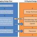
In my career in semiconductor industry, I can recall, in the beginning there was emphasis on design completion with automation as fast as possible. The primary considerations were area and speed of completion of a semiconductor design. Today, with unprecedented increase in multiple functions on the same chip and density of the… Read More
Xilinx announced their results today and had their conference call this afternoon, which I listened to. For them this is 1Q fiscal 2015 which means you have to be careful since there is a big difference between talking about fiscal quarters and calendar quarters. Xilinx’s conference calls are interesting for a couple of … Read More
Rather than watch the World Cup battle for third place, my beautiful wife and I spent last Saturday afternoon at the CASPA Wearables Symposium. The most interesting presentation was from Samsung because it included slides on their foundry offering. In regards to wearables, I still don’t see the ROI I need to buy one, yet. We are getting… Read More
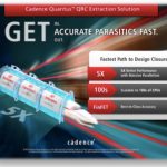
Today Cadence announced their next generation extraction solution called Quantus QRC. Actually they are technically announcing it tomorrow, since it is being announced at CDNLive in Korea where it is already Tuesday morning.
As with the other recently announced tools that end in -us, Tempus (timing signoff) and Voltus (power… Read More
There is an interesting article on Seeking Alpha about Intel. Interesting because it is written by someone with both fabless semiconductor experience and a talent for strategic thinking. It’s a good read and like most Seeking Aplha semiconductor articles the comments are hilarious. Give the guy a penny and click over HERE, he … Read More
One of the most interesting demos at #51DAC was the eSilicon GDS II online quote system for TSMC. Probably because eSilicon was one of the most interesting companies exhibiting this year. While writing the book “Fabless: The Transformation of the Semiconductor Industry” we took a close look at the history of fabless semiconductor… Read More
Cliff Hou had two major appearances at DAC this year. He gave the opening day keynote…and he wrote the forward to Dan and my bookFabless: the Transformation of the Semiconductor Industry which about 1500 lucky people got a copy of courtesy of several companies, most notably eSilicon who sponsored the Tuesday evening post-conference… Read More