

On Sunday I attended an IP workshop which was presented by TSMC, Atrenta, Sonics and IPextreme. It turns out that the leitmotiv of the afternoon was SpyGlass.
Dan Kochpatcharin of TSMC was first up and gave a little bit of history of the company. They built up their capacity over the years, as I’ve written about before, and last year shipped 15 milliion 8″ equivalent wafers. That’s a lot.
Ten years ago, TSMC could pretty much get away with throwing out the Spice rules and the DRC rules and letting design teams have at it. That no longer works because the complexity of the process means that each generation needs the tool chain to be adapted (for example, double patterning at 20nm) and nobody, even the biggest fabless guys, designs every block on their chip. IP for the process needs to be ready, especially memories, DDRx controllers, Ethernet and so on.
So TSMC started the IP alliance in 2000 for hard IP. Each block is tracked through a qualification process that starts with physical review (it must pass DRC or…fail), DRM compliance (ditto), pre-silicon assessment (design kit review), typical silicon assesment (tapeout review), split lot assessment, IP validation (characterization) and volume production (tracking customer use and yield). They have about 10,000 IP blocks in the system of which 1500 had problems, 373 of which were serious enough that they would have potentially been fatal. When a mask set costs $10M that is $3.7B in saved mask charges alone.
In 2010 they extended the program to soft IP (RTL level) working with Atrenta SpyGlass as the signoff tool. In the first go around, they focused on whether the RTL was correct and clean enough to pass Atrenta’s Lint checks, make sure the clocks were correct and so on. By the second version, using SpyGlass physical they were on the lookout for potential congestion and timing problems.
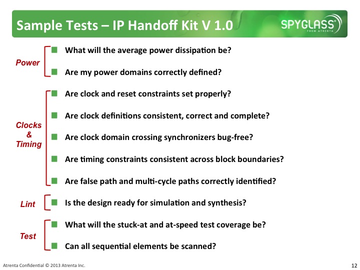
Next up was Mike Gianfagna from Atrenta. The focus of Atrenta at DAC this year is that the tools are now ready for RTL signoff. This doesn’t replace post-layout signoff which will still be required and it certainly doesn’t imply that design closure will simply happen without any manual intervention and ECOs. But it can catch a lot of problems early and ensure that the physical design process goes smoothly. The big advantages of working at the RTL level are twofold. Firstly, when problems are found they are much easier to address. And secondly, the tools (SpyGlass and others) run orders of magnitude faster than at the netlist or physical levels.
Run time would not matter if there was not good correlation between what SpyGlass predicted at the RTL level and what reality turned out to be post-layout. The most mature part of Atrenta’s technology is in the test area where they have been working for over 10 years. The prediction for stuck-at fault coverage at the RTL level is 1% off from the final numbers; for at-speed it is 2%. Power is more like 10%, area 5-10% and so on.
Atrenta/TSMC’s IPkit is now used by all partners in TSMC’s IP program. There are twice as many partners involved at this years DAC as were in 2012. IPkit 3.0 will add BugScope assertion synthesis to get better IP verification scripts.
After a brief break for coffee it was Sveta Avagyan of Sonics. She had been given a little design using IPextreme IP based around a Coldfire processor (68000 architecture). Sonics has various different interconnect and network-on-chip (NoC) technologies. Sveta showed us how to use the GUI to configure the whole subsystem interconnect. She could then use SpyGlass to make sure it was clean. Things that SpyGlass calls out as errors may, in fact, be OK and so one way to fix a problem is to issue a waiver that says it is actually OK. SpyGlass will record the waiver and track it all the way through the design process. Eventually, when the design is ready, it can be used in a chip or uploaded to IPextreme’s cloud-based infrastructure Xena.
Warren Savage discussed how Xena makes it easy for IP creators to upload designs, either fixed or parameterizable, to the cloud and for users to download them. However, Xena can also run SpyGlass (in the cloud) to produce reports on the quality of the IP, record waivers and so on.
So SpyGlass is now the de facto standard for IP quality. TSMC uses it for their soft IP program, IP providers such as Sonics can use it during IP creation (whether this is manual or something closer to compiler generated like Sonics), IPextreme can use it to qualify IP. Users can pull down some of the reports or run SpyGlass themselves on IP before deciding finally whether to use it or not. Everyone wants their IP to by SpyGlass clean (and that IPextreme and TSMC are happy with the quality too, not to mention their actual users).


Podcast EP357: How Gonka is Changing the Way AI is Accessed with David Liberman