You are currently viewing SemiWiki as a guest which gives you limited access to the site. To view blog comments and experience other SemiWiki features you must be a registered member. Registration is fast, simple, and absolutely free so please,
join our community today!
As the complexity of modern System-on-Chip (SoC) designs continues to rise, achieving energy efficiency measured as performance per watt has become a crucial design goal. With the increasing demand for powerful, multifunctional chips, balancing performance with power consumption has become essential. Realistic workloads… Read More
The Design Automation Conference (DAC) is a premier event that focuses on the design and automation of electronic systems. It is an annual conference that has been held since 1964, making it one of the longest-running and most established events in the field of electronic design automation (EDA).
DAC offers outstanding training,… Read More
Dieter Therssen obtained his master’s degree in Electronics Engineering from KU Leuven in 1987. He started his career as a hardware design engineer, using IMEC’s visionary tools and design methodologies in the early days of silicon integration.
Since then, Dieter developed his career across many digital technologies,… Read More
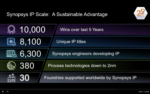
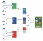
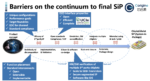
Semiconductor intellectual property (IP) plays a critical role in modern system-on-chip (SoC) designs. That’s not surprising given that modern SoCs are highly complex designs that leverage already proven building blocks such as processors, interfaces, foundational IP, on-chip bus fabrics, security IP, and others. This… Read More
The automotive industry is undergoing a remarkable transformation, with vehicles becoming more connected, automated, and reliant on software. While these advancements promise convenience, comfort and efficiency to the consumers, the nature and complexity of the technologies also raise concerns for functional safety … Read More
As I sift through mounds of semiconductor press releases trying to figure out the relevance (with mixed results) I consider it a learning experience even when they don’t really tell me anything. This one however tells me two very important things:
1) Arm is a much more competitive company with the new leadership. I saw a noticeable… Read More
The first chiplets focused summit took place last month. So many accomplished speakers gave keynote talks on what direction should and would the Chiplets ecosystem evolution take. Corigine presented the keynote on what direction hardware emulation should and would evolve for speeding up chiplet- based designs. During a pre-conference… Read More
Successful ASIC providers offer top-notch infrastructure and methodologies that can accommodate varied demands from a multitude of customers. Such ASIC providers also need access to best-in-class IP portfolio, advanced packaging and test capabilities, and heterogeneous chiplet integration capability among other things.… Read More
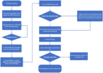
Introduction:
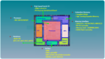
The advancements in deep submicron technology and adding multiple functionalities to reduce costs combined with scaling existing operations means that SoC designs become ever more complex. The biggest driving factors to go below the 16nm process node are the decrease in power and the increase in performance … Read More
This year is proving to be a momentous one for U.S. semiconductor manufacturing. During a global chip shortage and record inflation, President Biden signed into effect the CHIPS and Science Act – which so far is the greatest boon to U.S. semiconductor manufacturing in history, with $52 billion in subsidies for chip manufacturers… Read More