You are currently viewing SemiWiki as a guest which gives you limited access to the site. To view blog comments and experience other SemiWiki features you must be a registered member. Registration is fast, simple, and absolutely free so please,
join our community today!
At the #53DAC earlier this month held in Austin, Texas I met up with Renee Donkers, the founder of Fractal Technologies. His company has been focused on improving the quality of semiconductor IP cells through the use of automated checking software. The highest area of growth in EDA as measured by the ESD Alliance is in the reusable… Read More
Of late, it has become painfully obvious that the value of electronics is in the system. And since systems demand continuing improvement, increasing performance and decreasing cost (once partially guaranteed by semiconductor process advances) is now sought through algorithm advances – witness the Google TPU and custom… Read More
Top Ten #53DAC Highlightsby Tom Dillinger on 06-13-2016 at 12:00 pmCategories: EDA, Events
Here is a very subjective list of the Top 10 logistical and technical highlights from DAC’53.
(10) With DAC attendance down from its peak days, the Austin Convention Center served as an excellent venue. There was good participation from companies with design centers in the “Silicon Hills”. And, I saw colleagues from Silicon Valley,… Read More
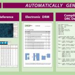
Design rules are at the heart of the interface between the foundry and semiconductor designers, which makes them so critical. Traditionally, design rules and DRC decks have been developed manually with no or little automation. Design rule definitions are written using WORD or other general purpose office tools, and DRC decks… Read More
If you’re headed to #53DAC (June 5-9 in Austin,TX) and are interested in learning more about FD-SOI, there will be lots of opportunities. Here’s a quick guide to get you started. … Read More
Continuing to find new ways to extend Moore’s Law, the foundry and technology leader is ready to show off its wafer level system integration prowess with two scalable platforms targeting key growth markets.
CoWoS® (Chip-On-Wafer-On-Substrate) goes after high-performance applications, providing the highest bandwidth and… Read More
Design starts are critical to the growth of the semiconductor industry so enabling them is a common theme on SemiWiki. One thing we have not covered in detail is multi-project wafer services (MPW) which is the equivalent of ride sharing through the initial mask and wafer process. Larger semiconductor companies already do this … Read More
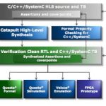
A common SoC design methodology in current use starts with preparation of the physical floorplan — e.g., block/pin placement, global clock domain and bus signal planning, developing the global/local power distribution (and dynamic power domain management techniques). Decoupling capacitor estimated densities and… Read More
If you plan on visiting Solido (the world leader in EDA software for variation-aware design of integrated circuits) at the Design Automation Conference next month for a demonstration of Variation Designer, register online now and get an autographed copy of “Mobile Unleashed”. Such a deal!
Solido Variation Designer is used by… Read More
If you look back at the beginning of the ASIC business you will see that it was really a critical time in the semiconductor industry. It all began in the 1980s which coincidentally is when I started my career in Silicon Valley. General purpose integrated circuits ruled the market, forcing system designers to cobble together off-the-shelf… Read More