You are currently viewing SemiWiki as a guest which gives you limited access to the site. To view blog comments and experience other SemiWiki features you must be a registered member. Registration is fast, simple, and absolutely free so please,
join our community today!
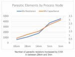
With advanced semiconductor processes continuing to shrink, the number and complexity of parasitic elements in designs grows exponentially contributing to one of the most significant bottlenecks in the design flow. Undetected parasitic-induced issues can be extremely costly, often resulting in tape-out delays.
Silvaco… Read More
High-speed PCB designs are complex, often requiring a team with design engineers, PCB designers and SI/PI engineers working together to produce a reliable product, delivered on time and within budget. Cadence has been offering PCB tools for many years, and they recently wrote a 10-page white paper on this topic, so I’ll share … Read More
The goal of SoC design teams is to tape-out their project and receive working silicon on the first try, without discovering any bugs in silicon. To achieve this lofty goal requires all types of specialized checking and verification during the design phase to prevent bugs. There are checks at the system level, RTL level, gate level,… Read More
At the beginning of every project the one of the first questions that ought to be asked is whether there blocks from previous designs that can be reused. On the surface this seems pretty obvious. The wrinkle in this is that reusability varies a lot based on the design type and the effort that a team is willing to expend to bring a design… Read More
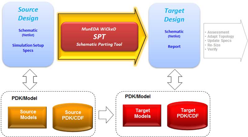
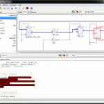
Schematics are still the lynchpin of analog design. In the time that HDL’s have revolutionized digital design, schematics have remained drawn and used much as they have been for decades. While the abstraction of HDL based designs has made process and foundry porting relatively straightforward, porting schematic based designs… Read More
This year is most notably the 50th anniversary of Moore’s Law. It is also the 25th anniversary of Concept Engineering. They were founded in 1990 in Freiburg Germany. They started by providing automatic schematic generation from netlist. They sold primarily to other EDA companies and to internal development groups in semiconductor… Read More
During SNUG I took the opportunity to chat to Choon-Hoe Yeoh of Lattice Semiconductor about how they use Concept Engineering’s Starvision Pro product. He is the senior director of EDA tools and methodologies there.
Lattice Semiconductor is a manufacturer of low-power, small-footprint, low-cost programmable logic devices.… Read More
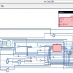
In the late 1990s I was the VP Engineering at Ambit Design Systems. We had a synthesis product (called BuildGates, nobody ever forgot the name). Both our own engineers and our customers wanted to be able to take a look at the gate-level netlist that was generated from their RTL. We used a product from a company called Concept Engineering… Read More
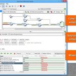
SoC design these days has become a complex and tricky phenomenon involving integration of multiple IPs and legacy RTL code which could be in different languages, sourced from various third parties across the globe. Understanding and reusing RTL code is imperative in SoC integration which needs capable tools that can accommodate… Read More
These days it’s common to expect large digital designs, analog blocks, custom IPs, glue logic, interfaces and interconnects all developed separately, perhaps by different vendors / teams, but integrated together in a single environment forming an SoC. The SoC can have multiple clock domains and can work in multiple modes of … Read More