Synopsys has been quite active lately in their messaging around formal verification. One such event at DVCon this year was a tutorial on some of the more advanced techniques/ methodologies that are accessible to formal teams, mostly presented by customers, though opened by a Synopsys presentation. The tutorial covered so many… Read More
Tag: samsung
Leading Edge Logic Landscape 2018
The most viewed blogs I write for SemiWiki are consistently blogs comparing the four leading edge logic producers, GLOBALFOUNDRIES (GF), Intel, Samsung (SS) and TSMC. Since the last time I compared the leading edge new data has become available and several new processes have been introduced. In this blog I will update the current… Read More
LithoVision 2018 The Evolving Semiconductor Technology Landscape and What it Means for Lithography
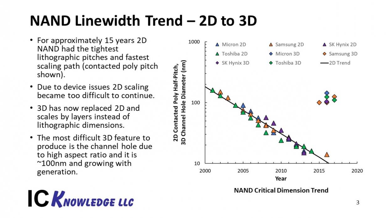
I was invited to present at Nikon’s LithoVision event held the day before the SPIE Advanced Lithography Conference in San Jose. The following is a write up of the talk I gave. In this talk I discuss the three main segments in the semiconductor industry, NAND, DRAM and Logic and how technology transitions will affect lithography.… Read More
IEDM 2017 – Leti Gate-All-Around Stacked-Nanowires
At IEDM in December I had a chance to interview Thomas Ernst about the paper “Performance and Design Considerations for Gate-All-around Stacked-NanoWires FETs” by Leti and STMicroelectonics.
Leti published the first stacked nanowire in 2006, it was very new then, now stacked nanowire/nanosheets are starting… Read More
IEDM 2017 – Controlling Threshold Voltage with Work Function Metals
As I have said many times, IEDM is one of the premier conferences for semiconductor technology. On Sunday before the formal conference started I took the “Boosting Performance, Ensuring Reliability, Managing Variation in sub-5nm CMOS” short course. The second module in the course was “Multi-Vt Engineering… Read More
ISS 2018 – The Impact of EUV on the Semiconductor Supply Chain
I was invited to give a talk at the ISS conference on the Impact of EUV on the Semiconductor Supply Chain. The ISS conference is an annual gathering of semiconductor executives to review technology and global trends. In this article I will walk through my presentation and conclusions.… Read More
IEDM 2017 – Intel Versus GLOBALFOUNDRIES at the Leading Edge
As I have discussed in previous blogs, IEDM is one of the premier conferences to learn about the latest developments in semiconductor technology. … Read More
IP-SoC 2017: IP Innovation, Foundries, Low Power and Security
The 20[SUP]th[/SUP] IP-SoC conference will be held in Grenoble, France, on December 6-7, 2017. IP-SoC is not just a marketing fest, it’s the unique IP centric conference, with presentations reflecting the complete IP ecosystem: IP suppliers, foundries, industry trends and applications, with a focus on automotive. It will … Read More
Choosing the lesser of 2 evils EUV vs Multi Patterning!
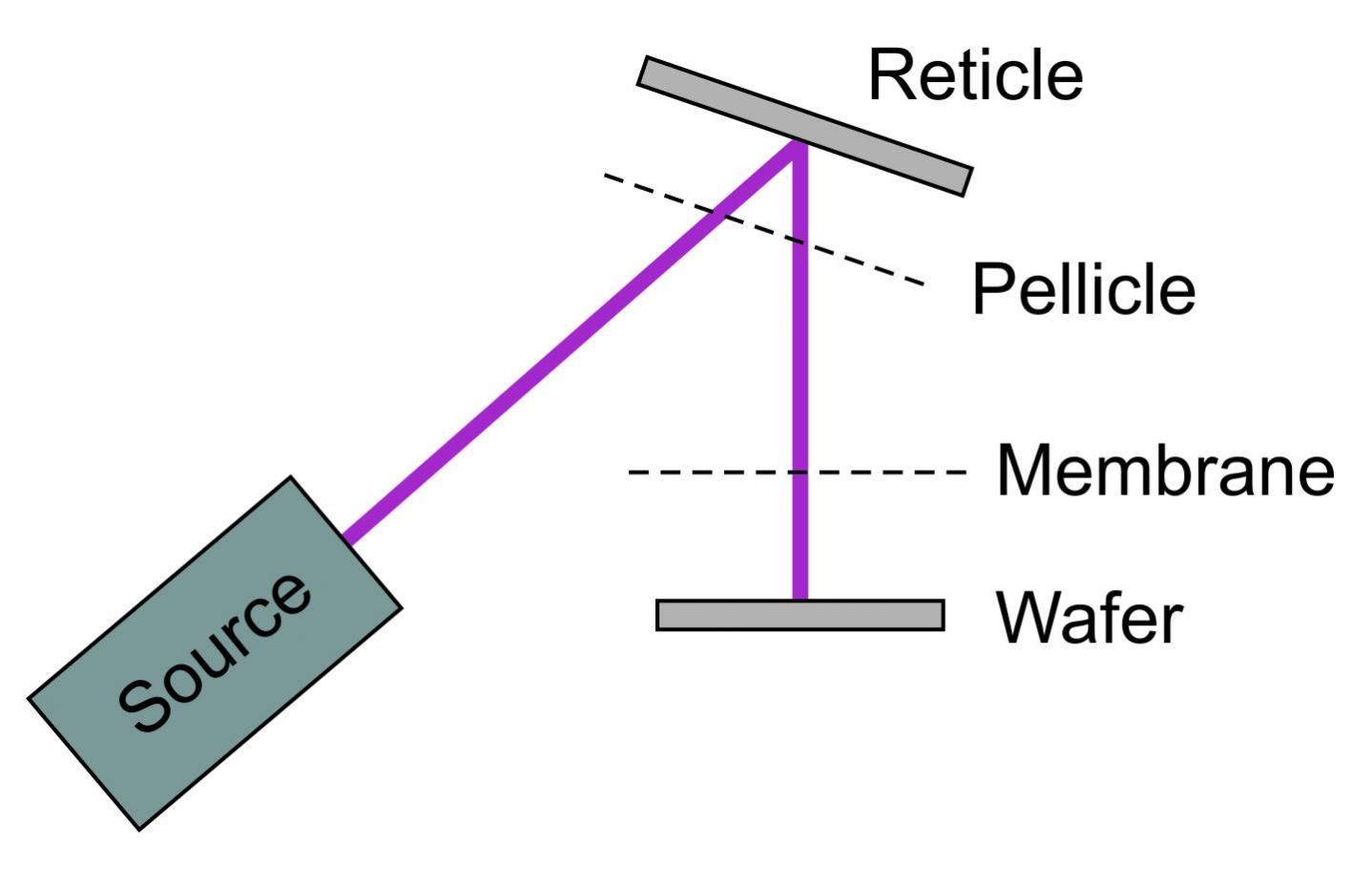
For Halloween this week we thought it would be appropriate to talk about things that strike fear into the hearts of semiconductor makers and process engineers toiling away in fabs. Do I want to do multi-patterning with the huge increase in complexity, number of steps, masks and tools or do I want to do EUV with unproven tools, unproven… Read More
Deal Struck for Sale of Toshiba NAND to Bain Apple and Others
What does it mean for the skyrocketing memory sector? In a last minute plot twist, Bain capital appears to be the winner in the auction of the Toshiba memory unit. The Bain consortium includes a strange cast of characters including Apple, Dell, Seagate, Kingston Technology, Innovation Network Corp of Japan and Development Bank… Read More


