You are currently viewing SemiWiki as a guest which gives you limited access to the site. To view blog comments and experience other SemiWiki features you must be a registered member. Registration is fast, simple, and absolutely free so please,
join our community today!
Semiconductor stocks have had another significant down leg as the bad news continues to pile on. Bad news in this case doesn’t come in threes , it comes in droves. TI is perhaps very scary news as it is a rather broad based supplier of semiconductors that has fared better than more pure play chip suppliers. TI gave weak guidance… Read More
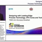
One of my favorite traditions at the Design Automation Conference is the Synopsys foundry events (the videos are now available). I learned a long time ago that the foundries are the foundation of the fabless semiconductor ecosystem and your relationships with the foundries can make or break you, absolutely. I also appreciate … Read More
Applied reported a more or less in line quarter, slightly beating weaker expectations. As we had projected, the October quarter is expected to have revenues down 10% which is at the low end of our expected 10-15% drop in business. Applied services helped partially make up for some of the equipment sales weakness. Revenue came in … Read More
Applied Materials (AMAT) is batting clean up in a quarter that has not been pretty. Lately semi stocks seem to have been hit by not only stock specific issues but continued and increasing memory concerns coupled with more macro issues. On top of all this, China trade issues which have in the meantime taken a back burner to other issues… Read More
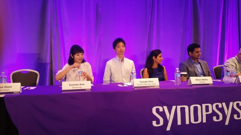
At #55DAC in SFO the first day is always the busiest on the exhibit floor, so Monday by lunch time I was hungry and took a short walk to the Marriott hotel nearby to listen to AMS experts from several companies talk about their EDA tool use, hosted by Synopsys:
- Samsung
- Toshiba Memory Corp.
- NVIDIA
- Seagate
- Numem
- Esperanto
…
Read More
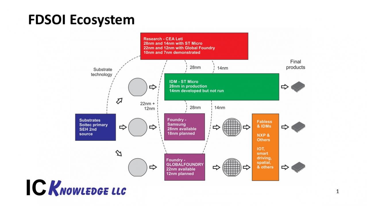
FDSOI is gaining traction in the market place. At their foundry forum in May, Samsung announced they have 17 FDSOI products in high volume manufacturing (you can read Tom Dilliger’s write up of the Samsung Foundry Forum here). At SEMICON West in July, GLOBALFOUNDRIES (GF) announced FDSOI design wins worth $2 billion dollars in … Read More
A variety of growing and emerging segments of the semiconductor industry rely on Silicon-On-Insulator (SOI) wafers. Soitec is the primary source for SOI wafers particularly on 300mm. On Tuesday at SEMICON I got to sit down with Bernard Aspar, Soitec’s Executive Vice President, Communication & Power BU and Christophe… Read More
We attended Semicon West Monday and Tuesday, the annual show for the semi equipment industry. Its very clear from discussions with all our sources in the industry that confirm that Samsung has put the brakes on spending on memory and that message was reinforced by declines in their expected profitability due to weaker memory pricing.… Read More
There has been a lot of new information available about the leading-edge logic processes lately. Papers from IEDM in December 2017, VLSIT this month, the TSMC and Samsung Foundry forums, etc. have all filled in a lot of information. In this article I will summarize what is currently known.… Read More
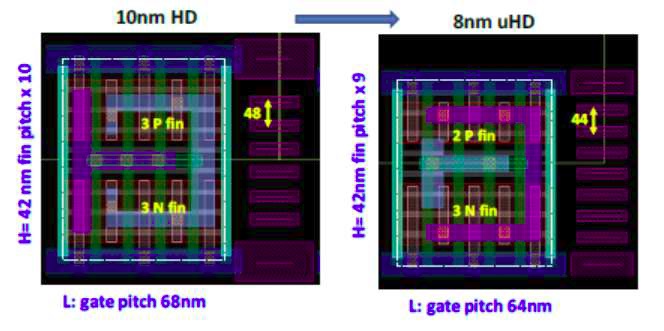
I got a tip sheet today for the upcoming 2018 Symposia on VLSI Technology & Circuits to be held June 19th through 21st in Honolulu, Hawaii. There is some interesting information on Samsung’s 10nm, 8nm and 7nm processes in the tip sheet:… Read More