The server market is a diverse, yet standardized market. The ICs and components designed and manufactured in final assemblies must meet form factor requirements for rack mount and blades. The form factor enclosures and the component placement dictate the thermal-mechanical properties and hence the thermal cooling limits … Read More

Tag: rtl
Automatic RTL Restructuring: A Need Rather Than Convenience
In the semiconductor design industry, most of the designs are created and optimized at the RTL level, mainly through home grown scripts or manual methods. As there can be several iterations in optimizing the hierarchy for physical implementation, it’s too late to do the hierarchical optimizations after reaching the floor plan… Read More
How to Reduce Maximum Power at RTL Stage?
Of course that reduction has to stay throughout the design cycle up to layout implementation and fabrication. Since the advent of high density, mega functionality SoC designs at advanced nodes and battery life critical devices played by our fingertips, the gap between SoC power requirement and actual SoC power has only increased.… Read More
Accelerating SoC Verification Through HLS
Once upon a time there was a struggle for verification completion of semiconductor designs at gate level. Today, beyond imagination, there is a struggle to verify a design with billions of gates at the RTL level which may never complete. The designs are large SoCs with complex architectures and several constraints of area, performance,… Read More
Concept Engineering Showcases Effective SoC Debugging Techniques

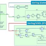
In a complex environment of semiconductor design where an SoC can have several millions of gates and multiple number of IPs at different levels of abstractions from different sources integrated together, it becomes really difficult to understand and debug the overall SoC design. Of course, along with the SoC integration, optimization… Read More
Ten Innovative Debugging Techniques – Pre & Post Layout
In a complex world of SoCs with multi-million gates and IPs from several heterogeneous sources, verification of a complete semiconductor design has become extremely difficult, and it’s not enough. In order to ascertain the right intent of the design throughout the design cycle, debugging at various stages of the design cycle… Read More
Expert Constraint Management Leads to Productivity & Faster Convergence
The SoC designs of today are much more complex than ever in terms of number of clocks, IPs, levels of hierarchies, several modes of operations, different types of validations and checks for growing number of constraints at various stages in the design flow. As a semiconductor design evolves through several stages from RTL to layout,… Read More
Mark your Date for Semiconductor Design Vision
A very popular acronym is ‘WYSIWYG’ – What You See Is What You Get! This is very true and is important to visualize things to make it better in various aspects such as aesthetics, compactness, organization, structure, understandable for correction and so on; the most important, in case of semiconductor design, is being able to identify… Read More
How to meet 3Ps in 3D-ICs with sub-20nm Dies?

It feels to be at the top of semiconductor technology by having dies with high density of semiconductor design at sub-20nm technology node stacked together into a 3D-IC to form a complete SoC which can accommodate billions of gates. However there are multiple factors to be looked at in order to make that successful amid often conflicting… Read More
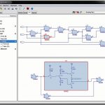
Mixed-Signal SoC Debugging & IP Integration Made Easy
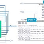
A semiconductor SoC design can have multiple components at different levels of abstractions from different sources and in different languages. While designing an SoC, IPs at different levels have to be integrated without losing the overall design goals. Of course, quality of an IP inside and outside of an SoC must be tested thoroughly.… Read More