You are currently viewing SemiWiki as a guest which gives you limited access to the site. To view blog comments and experience other SemiWiki features you must be a registered member. Registration is fast, simple, and absolutely free so please,
join our community today!
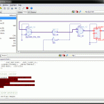
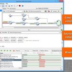
During SNUG I took the opportunity to chat to Choon-Hoe Yeoh of Lattice Semiconductor about how they use Concept Engineering’s Starvision Pro product. He is the senior director of EDA tools and methodologies there.
Lattice Semiconductor is a manufacturer of low-power, small-footprint, low-cost programmable logic devices.… Read More
With High-Level Synthesis (HLS) the first benefit that comes to my mind is reduced design time, because coding with C or SystemC is more efficient than low-level RTL code. What I’ve just learned is that there’s another benefit, a reduction in the amount of functional simulation required. One HLS customer was able … Read More
SoC design these days has become a complex and tricky phenomenon involving integration of multiple IPs and legacy RTL code which could be in different languages, sourced from various third parties across the globe. Understanding and reusing RTL code is imperative in SoC integration which needs capable tools that can accommodate… Read More
Last week I was traveling in Munich attending the MunEDA User Group meetingso I missed a live webinar on the topic of optimizing for power at RTL. I finally got caught up in my email this week and had time to view this 47 minute webinar, presented by Guillaume Boilletof Atrenta. He recommended using a combination of automatic, semi-automatic… Read More
For about a decade I am looking forward to seeing more of system level design and verification including high level synthesis (HLS), virtual prototyping, and system modeling etc. to come in the main stream of SoC design. Although the progress has been slow, I see it accelerating as more and more tools address the typical pain points… Read More
These days it’s common to expect large digital designs, analog blocks, custom IPs, glue logic, interfaces and interconnects all developed separately, perhaps by different vendors / teams, but integrated together in a single environment forming an SoC. The SoC can have multiple clock domains and can work in multiple modes of … Read More
In a semiconductor design, keeping the design testable with high test coverage has always been a requirement. However with shrinking technology nodes and large, dense SoC designs and complex logic structures, while it has become mandatory to reach close to 100% test coverage, it’s extremely difficult to cope with the explosion… Read More
I think by now there has been good level of discussion on FinFET technology at sub-20 nm process nodes and this is an answer to ultra dense, high performance, low power, and billion+ gate SoC designs within the same area. However, it comes with some of the key challenges with respect to power, noise and reliability of the design. A FinFET… Read More
Very recently, I was seeing intense discussions on the need for agile hardware development just like agile software and ideas were being sought from experts as well as individuals. While in software world it has already evolved, in hardware world it’s yet to see the shift in paradigm. My point is that the end goal of agile hardware… Read More
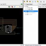
In today’s SoC world where multiple analog and digital blocks along with IPs at different levels of abstractions are placed together on a single chip, debugging at all levels becomes quite difficult and clumsy. While one is working at the top level and needs to investigate a particular connection at an intermediate hierarchical… Read More