You are currently viewing SemiWiki as a guest which gives you limited access to the site. To view blog comments and experience other SemiWiki features you must be a registered member. Registration is fast, simple, and absolutely free so please,
join our community today!
Power delivery networks (PDN) are the metal structures on a chip that delivers the power. In a high-end desktop SoC this might be delivering as much as 150W, and with voltages around 1V that means over 150 amps of current. Clearly getting the PDN correct is critical for a correctly functioning chip. One of the challenges to verifying… Read More
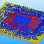
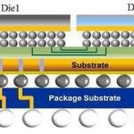
3D-IC has a stack of dies connected and packaged together, and therefore needs new testing strategies other than testing a single die. It’s given that a single defective die can render the whole of 3D-IC unusable, so each die in the stack must be completely and perfectly tested before its entry into that stack. Looking at it from a … Read More
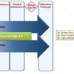
Are you a TSMC customer or partner? If so, you’ll want to take a look at these presentations from the 2013 TSMC Open Innovation Platform conference:
…
Read More
When we talk about parasitic, we talk about post layout design further expanded in terms of electrical components such as resistances and capacitances. In the semiconductor design environment where multiple parts of a design from different sources are assembled together into highly complex, high density SoC, imagine how complex… Read More
I met with Tom Quan of TSMC and Michael Beuler-Garcia of Mentor last week. Weirdly, Mentor’s newish buildings are the old Avant! buildings where I worked for a few weeks after selling Compass Design Automation to them. Odd sort of déja vu. Historically, TSMC has operated with EDA companies in a fairly structured way: TSMC … Read More
This is obviously great news for SilabTech, and this is the type of news which will change the perception that we (non-Indian) have of the Semiconductor industry in India. About 15-20 years ago, the India Embedded/VLSI industry was perceived as low cost design resource pool, a good place where to implement design center. The hidden… Read More
In most of the electronic equipments, semiconductor chips are a major source of heat generation. And in semiconductor designs several hardware and software techniques are being used to contain power dissipation; a major cause for heat. However due to multiple functionality being squeezed into small form factors, we continue… Read More
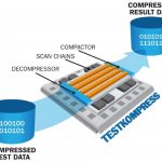
As we move down into more and more advanced process nodes, the rules of how we test designs are having to change. One big challenge is the requirement to zoom in and fix problems by doing root cause analysis on test data alone, along with the rest of the design data such as detailed layout, optical proximity correction and so on. But without… Read More
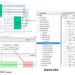
One of the challenges of physical design of a modern SoC is that of macro placement. Back when a design just had a few macros then the flooplanning could be handled largely manually. But modern SoCs suffer from a number of problems. A new white paper from Mentor covers Olympus-SOCs features to address these issues:
…
Read More
Traditionally ATPG (Automatic Test Pattern Generation) and BIST (Built-In-Self-Test) are the two approaches for testing the whole semiconductor design squeezed on an IC; ATPG requires external test equipment and test vectors to test targeted faults, BIST circuit is implemented on chip along with the functional logic of IC.… Read More