You are currently viewing SemiWiki as a guest which gives you limited access to the site. To view blog comments and experience other SemiWiki features you must be a registered member. Registration is fast, simple, and absolutely free so please,
join our community today!
One of the privilages of blogging for SemiWiki is invitations to the top conferences around the world including the International Solid-State Circuits Conference (ISSCC) in San Francisco this week. Amazing, this conference is older than I am:
ISSCC 2013 is the 60th Conference in an incredibly long-lasting series. Following… Read More
Tubes of the Futureby Paul McLellan on 02-07-2013 at 10:00 pmCategories: General
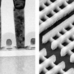
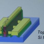
So what is a silicon nanowire? It is basically a FET where the active element is a wire 3-20nm in diameter. So where a FinFET has the gate wrapped around 3 sides of the transistor, a nanowire (NW) has it wrapped around all four. In essence, the wire runs through the middle of the gate.
There seem to be three issues about building a silicon… Read More
Can’t make it to Santa Clara? Join us online!
The detailed 2013 CPTF agenda is now up in preparation for the February 5th event at the Santa Clara Convention Center. This is one of the rare times that you can get a free lunch! Watch this quick video to see what is in store for us this year. Dr. Paul McLellan and I will be there so please… Read More
I spent some quality time with Subi Kengeri, Vice President, Technology Architecture, Office of the CTO, GLOBALFOUNDRIES in Las Vegas during CES. Great guy, he worked at Silicon Access, Virage and TSMC before GF. One thing you should know about embedded memory guys, SRAM is the first thing that goes through a new process so they … Read More
This is the second blog entry about an ST Ericsson white-paper on multiprocessors in mobile. The first part was here.
The first part of the white-paper basically shows that for mobile the optimal number of cores is two. It is much better to use process technology (and good EDA) to run the processor at higher frequency rather than add… Read More
The biggest surprise embedded in the Intel 22nm SoC disclosure is that they still do NOT use Double Patterning which is a big fat hairy deal if you are serious about the SoC foundry business. The other NOT so surprising thing I noticed in reviewing the blogosphere response is that the industry term FinFET was dominant while the Intel… Read More
In 2012 FinFET is one of the most talked about MOS technologies of the year because traditional planar CMOS has slowed down on scaling below the 28nm node. To learn more about FinFET process modeling I attended a Synopsys webinar where Bari Biswas presented for about 42 minutes include a Q&A portion at the end.
Bari Biswas, Synopsys… Read More
Introduction to FinFET Technology Part IIIby Tom Dillinger on 11-21-2012 at 5:30 pmCategories: FinFET, General
The preceding two Semiwiki articles in this thread provided an overview to the FinFET structure and fabrication. The next three articles will discuss some of the unique modeling requirements and design constraints that FinFET’s introduce, compared to planar FET technology.
Due to the complexity of FinFET modeling – … Read More
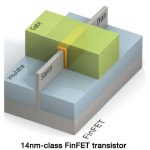
The common theme amongst semiconductor ecosystem conferences this year is FinFETS, probably the most exciting technology we will see this decade. A lot has been written on SemiWiki about FinFETS, it is one of the top trending search terms, but there is some confusion about the process naming so let me attempt to explain.
In planar… Read More
An announcement at the ARM conference was of a joint project to tape out an ARM Cortex-M0 in IBM’s 14nm FinFET process. In fact they taped out 3 different versions of the chip using different routing architectures to see the impact on yield.
This was the first 14nm ARM tapeout, it seems. I’m sure Intel has built plenty … Read More