You are currently viewing SemiWiki as a guest which gives you limited access to the site. To view blog comments and experience other SemiWiki features you must be a registered member. Registration is fast, simple, and absolutely free so please,
join our community today!
Intel is the number one semiconductor company in the world and has taken the lead in bringing FinFET (aka Tri-Gate) silicon to market at the 22nm node starting in May 2011, so now we see the pure play foundries playing catch-up and start talking about their own FinFET roadmaps. IC designers and layout engineers want to know how their… Read More
Today GlobalFoundries announced a 14nm process that will be available for volume production in 2014. They are explicitly trying to match Intel’s timeline for the introduction of 14nm. The process is called 14XM for eXtreme Mobility since it is especially focused on mobile. The process will be introduced just one year after… Read More
Thanks to SemiWiki readers for the feedback and comments on the previous “Introduction to FinFET Technology” posts – very much appreciated! The next installment on FinFET modeling will be uploaded soon.
In the interim, Dan forwarded the following link to me “ Intel’s FinFETs too complicated and difficult, says … Read More
Rajiv Bhateja, Dhrumil Gandhi and Neal Carney met with me at DAC on Wednesday to give an update on what’s new in 2012 for Tela Innovations, a provider of lithography optimized IP and tools. This team has a rich history in EDA and IP from companies like: ARM, Artisan, Mentor Graphics and Silicon Compilers.… Read More
Ever since the “Intel Reinvents Transistors Using New 3-D Structure” PR campaign I have been at odds with them. As technologists, I have nothing but respect for Intel. The Intel PR department, however, quite frankly, is evil. Correct me if I’m wrong here but Intel did not “reinvent” the transistor. Nor did they come up with the name… Read More
Clever title but it’s not mine. Piper Jaffray Analysts Auguste Richard and Jennifer Baxter released a report last week which echoed the concerns of others, including myself. The concerns reported are with the 22nm process and not the chipsets themselves. To me this is all part of ramping a leading edge process but the concerns are… Read More
Since the last Intel logo parody went over so well here is another one! Not so much a parody in light of the recent PR from Intel that the fabless semiconductor business model is doomed. As one of the doomed little people inside the fabless ecosystem I take exception to this but I digress….
The word around Silicon Valley is that Intel … Read More
Perhaps the most pertinent comment raised by an analyst at Intel’s Investor Forum last week came from Dan Hutcheson of VLSI Research to Brian Krzanich, the COO and head of global manufacturing and supply chain. He said: “I think you sold yourself short on Trigate, the benefit of fully depleted vs. planar and the impact on leakage.”… Read More
We have all heard that planar transistors have run out of steam. There are two ways forward. The one that has garnered all the attention is Intel’s trigate which is their name for FinFET. The other is using thin film SoI which ST is doing. TSMC and Global seem to be going the FinFET way too, although at a more leisurely pace. But … Read More
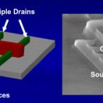
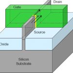
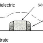
The previous post in this series provided an overview of FinFET devices. This article will briefly cover FinFET fabrication.
The major process steps in fabricating silicon fins are shown in Figures 1 through 3. The step that defines the fin thickness uses Sidewall Image Transfer (SIT). Low-pressure chemical vapor (isotropic)… Read More