You are currently viewing SemiWiki as a guest which gives you limited access to the site. To view blog comments and experience other SemiWiki features you must be a registered member. Registration is fast, simple, and absolutely free so please,
join our community today!
I will be at Semicon West from 9th to 11th July in Moscone, San Francisco. Of course there are lots of interesting sessions but here are two that I think are especially important to get a good impression of the way things are going in the future from experts. The two most interesting questions about the future are what comes after 14nm,… Read More
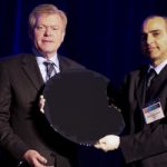
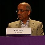
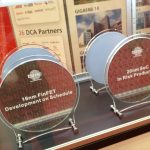
At DAC in Austin a design company, foundry and EDA vendor teamed up to present their experiences with 14nm FinFETs during a breakfast on Tuesday.
Panelists included:
…
Read More
This completely misleading title is from a Seeking Alpha (SA) article, a stock investment version of the National Enquirer. As I mentioned inA Call to ARMs, fame and fortune seeking SA Authors make a penny per click so sensationalism sells. The article is not worth your time so I will save you the click and skip to the misguided conclusion:… Read More
Lawsuits in EDA are common, and Tela Innovationsfiled a huge complaint back in February with the U.S. International Trade Commission (USITC) against HTC Corporation; HTC America, Inc.; LG Electronics, Inc.; LG Electronics U.S.A., Inc.; LG Electronics MobileComm U.S.A., Inc.; Motorola Mobility LLC; Nokia Corporation; Nokia,… Read More
Roaming the aisles at #50DAC the past week left me with one unmistakable impression: there were two shows going on at the same time. Oh, we were all packed into one space together at the Austin Convention Center and neighboring hotels. But we weren’t quite all speaking the same language – yet.… Read More
This year’s Kaufman award winner is Chenming Hu. In contrast to previous years, this was presented on the Sunday evening of DAC instead of at a separate event in San Jose. Chenming’s career was reviewed by Klaus Schuegraf, Group Vice President of EUV Product Development at Cymer, Inc (now part of ASML) and also one of… Read More
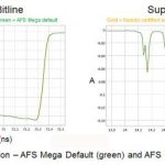
Berkeley Design Automation today announced the first silicon-accurate circuit simulation for mega-scale arrays like memories and CMOS image sensors. If this tool lives up to its claims, it is going to be a big deal for FinFET-based circuits, Memory designers are rightly worried about having the accuracy necessary to include… Read More
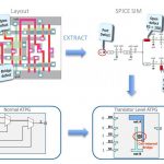
My 8 years as an IC circuit designer were at the transistor-level, so if that interests you as well then consider what there is to see from Cadence at DAC this year. IC design technology is changing quickly, so keeping up to date is important for your job security and continual education goals.
Here’s what I would recommend attending… Read More
Cell-Aware Test Seminarby Beth Martin on 05-07-2013 at 8:05 pmCategories: EDA, Siemens EDA
You may have heard about cell-aware testing. It’s a transistor-level test (ATPG) methodology that is quickly becoming a hot topic. If you are involved in DFT and are looking for better quality and reliability, you should definitely know about cell-aware testing.
And lucky you, on May 16, 2013, you can attend a free seminar on cell-aware… Read More
Mentor Graphics’ Best User2User Everby Beth Martin on 04-23-2013 at 5:45 pmCategories: EDA, Siemens EDA
Calling all Mentor users! Don’t forget to register for the U2U in San Jose on Thursday, April 25.
In addition to three worthy keynotes, you will find a more interactive and solution-focused day than in the past. There are sessions on place & route, custom/AMS, emulation, test and yield analysis, functional verification, Calibre… Read More