You are currently viewing SemiWiki as a guest which gives you limited access to the site. To view blog comments and experience other SemiWiki features you must be a registered member. Registration is fast, simple, and absolutely free so please,
join our community today!
One of the more frequent questions I get, “What is next after FinFETs?” is finally getting answered. Thankfully I am surrounded by experts in the process technology field including Scotten Jones of IC Knowledge. I am also surrounded by design enablement experts so I really am the man in the middle which brings us to a discussion between… Read More
On their first quarter earnings call Intel announced that volume production of 10nm has been moved from the second half of 2018 to 2019 due to yield issues. Specifically, they are shipping 10nm in low volume now, but yield improvement has been slower than anticipated. They report that they understand the yield issues but that improvements… Read More
Intel (INTC) blew away expectations based on strong performance in the data center. Revenues of $16.1B versus street of $15.05B and EPS of $0.93 versus street of $0.72. While revenue was up 9% over prior year, earnings were 50% higher. Guidance is for Q2 revenue of $16.3B and EPS of $0.85 versus street of $15.55B and EPS of $0.81. IOT,… Read More
TSMC warns soft phone/crypto & flat capex!
Does this impact DRAM?
Can Intel keep Apple?
We love Tesla (Model 3)!… Read More
ASML put up good results with revenues of Euro2.285B versus street of Euro2.22B and EPS of Euro1.26 versus street of Euro1.17. Guide is for Euro2.55B versus street of Euro2.46B but EPS of Euro1.16 versus street EPS of Euro1.35 on lower gross margins, slipping from 48% to 43%.
A couple of EUV systems have slipped out. This is not surprising… Read More
There is a report in the Seoul Economic Daily that Samsung has completed development of their 7nm process using EUV and that production will begin in June. What is claimed in the report is:
- The process is installed in the Hwaseong S3 Fab
- Samsung has more than 10 EUV systems installed
- Production starts in June with Qualcomm, Xilinx,
…
Read More
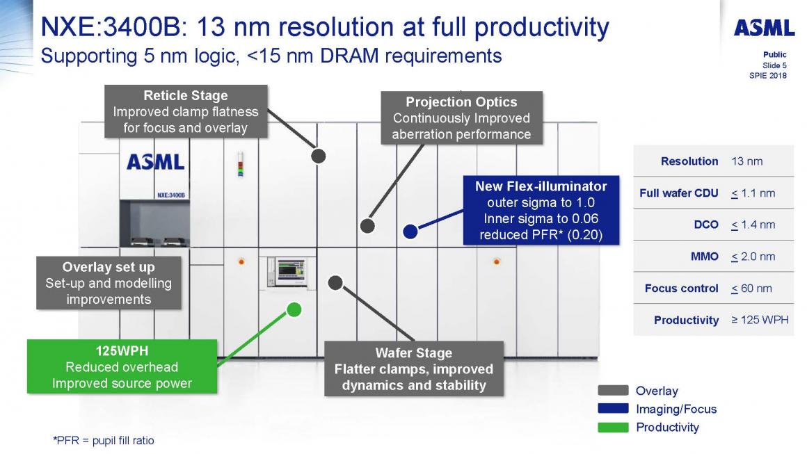
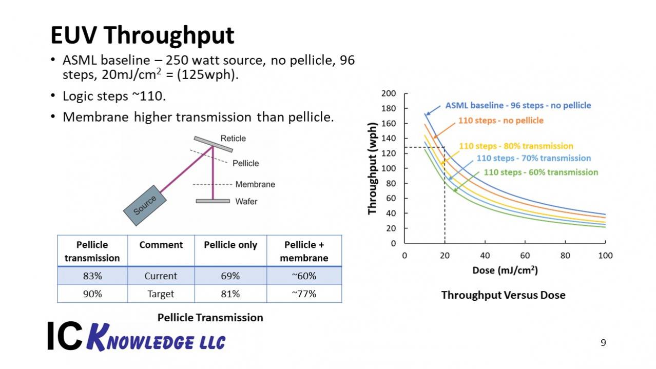
At the SPIE Advanced Lithography Conference in February ASML gave an update on their EUV systems, in this blog I will provide a summary of what they presented. I have also written about my impressions on EUV for the overall conference here.… Read More
This year the Advanced Lithography Conference felt very different to me than the last couple of years. I think it was Chris Mack who proclaimed it the year of Stochastics. EUV has dominated the conference for the last several years but in the past the conversation has been mostly centered on the systems, system power and uptime.
I … Read More
I was invited to give a talk at the ISS conference on the Impact of EUV on the Semiconductor Supply Chain. The ISS conference is an annual gathering of semiconductor executives to review technology and global trends. In this article I will walk through my presentation and conclusions.… Read More
For Halloween this week we thought it would be appropriate to talk about things that strike fear into the hearts of semiconductor makers and process engineers toiling away in fabs. Do I want to do multi-patterning with the huge increase in complexity, number of steps, masks and tools or do I want to do EUV with unproven tools, unproven… Read More