If you’ve followed my last article, The Guiding Light and Other Photonic Soaps, you read my comments about the use of waveguides to “guide the light” in photonic integrated circuits (PICs). This article continues the soap opera theme, this time with the Young and the Restless. My point here is that I am continually struck by the dichotomies… Read More

Tag: eda
"Re-Inventing" Tapeout Sign-off — Applying Big Data Techniques to Electrical Analysis
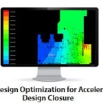
A common SoC design methodology in current use starts with preparation of the physical floorplan — e.g., block/pin placement, global clock domain and bus signal planning, developing the global/local power distribution (and dynamic power domain management techniques). Decoupling capacitor estimated densities and… Read More
Where are the Entrepreneurs?
This week I attended the UpWest Labs event in San Francisco. UpWest Labs provides seed funding and incubation for a wide range of domains including Enterprise Software, Internet of Things, Infrastructure Technologies, Artificial Intelligence, Consumer Applications, Drones, Cyber Security, Augmented Reality / Virtual … Read More
Getting Low Power Design Right in Mixed Signal Designs

Mixed-signal design creates all sorts of interesting problems for implementation and verification flows, particularly when it comes to design for low power. We tend to think of mixed-signal as a few blocks like PLLs, ADCs and PHYs on the periphery of the design. Constrain and verify the digital power requirements up to analog … Read More
CEO Insight: Transformation of Vayavya Labs into System Design Automation
With the advent of SoCs, design abstractions and verification has moved up at the system level. It’s imperative that EDA moves up the value chain to start design automation at system level. The System Design Automation will be the new face of EDA in coming years.… Read More
Seven Reasons to Attend DAC in Austin
I’m attending the 53rd Design Automation Conference (DAC) in Austin, Texas starting June 5th, and there are at least seven reasons that you should consider attending as well. For decades now DAC has been the premier place for all the players in our semiconductor ecosystem to get together: Academics, Commercial vendors … Read More
ARM and FD-SOI are like Peanut Butter and Jelly!
When I first heard about a foundry possibly licensing FD-SOI I would have bet it was SMIC in China. What better market for a low cost, low power, easy to manufacture alternative to FinFETs? The foundry of course was Samsung which also made complete sense since they have 28nm gate-first capacity that matches up nicely to 28nm FD-SOI.… Read More
Dr. Evil and On-Chip "LASERS" for Silicon Photonics
In the 1999 comedy, The Spy Who Shagged Me, Dr. Evil laments about why he can’t have sharks with “laser beams” attached to their heads. I get the feeling that silicon photonic designers sometimes feel the same way about why they don’t yet have integrated on-chip laser light sources. While off-chip light… Read More
3D TCAD Simulation of Silicon Power Devices
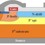
Process and device engineers are some of the unsung heroes in our semiconductor industry that have the daunting task of figuring out how to actually create a new process node that will fit some specific, market niche with sufficient yield to make their companies profitable and stand out from the competition. One such market segment… Read More
The Most Important Point You May Have Missed at CDNLive 2016!
This was the best keynote lineup I can remember at a user group meeting. All four speakers are visionaries but from very different perspectives. The video of the event will be up later this month but from my first count the word “System(s)” was mentioned 32 times and the underlying message will transform the semiconductor industry… Read More