You are currently viewing SemiWiki as a guest which gives you limited access to the site. To view blog comments and experience other SemiWiki features you must be a registered member. Registration is fast, simple, and absolutely free so please,
join our community today!
Each year, TSMC conducts two events – the Technology symposium in the Spring and the Open Innovation Platform (OIP) ® Ecosystem Forum in the Fall. Yet, what is the OIP ecosystem? What does it encompass? And, how does the program differentiate TSMC from other foundries? At the recent OIP Forum in Santa Clara, Suk Lee, Senior Director,… Read More
TSMC recently held their annual Technology Symposium in Santa Clara. Part 1 of this article focused on the semiconductor process highlights. This part reviews the advanced packaging technologies presented at the symposium.
TSMC has clearly made a transition from a “pure” wafer-level foundry to a supplier of complex integrated… Read More
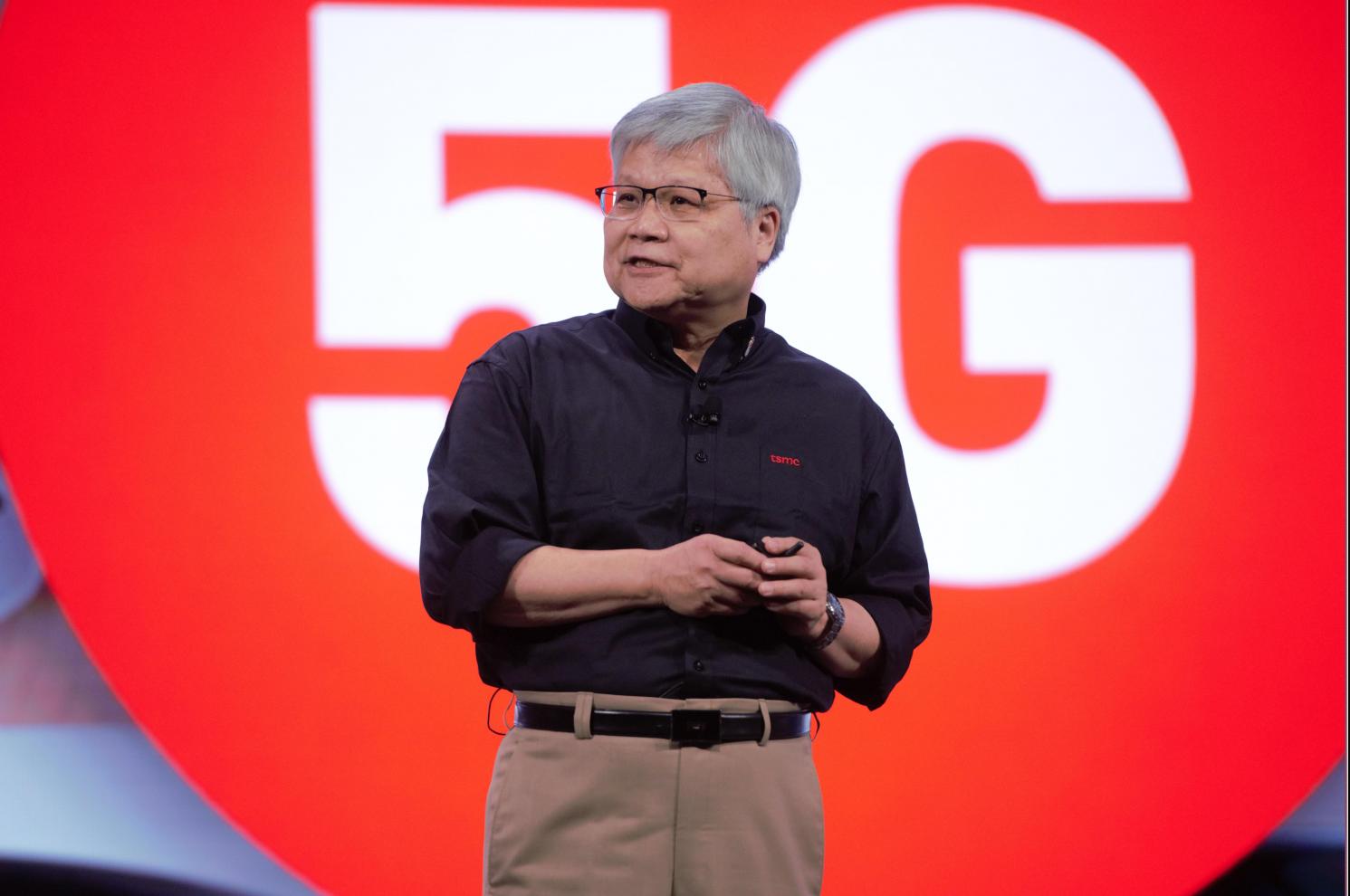
This year TSMC did a FinFET victory lap with the success of 16nm, 12nm, 10nm, and 7nm. It really is well deserved. Even though TSMC credits the ecosystem and customers, I credit TSMC and their relationship with Apple since it has pushed us all much harder than ever before. TSMC CEO C.C. Wei summed it up nicely in his keynote: Innovation,… Read More
The TSMC OIP Forum was very upbeat this year and now we know why. It wasn’t long ago that some media outlets and a competitor said 7nm would not be a popular node because it is too expensive blah blah blah. People inside the fabless semiconductor ecosystem however know otherwise. As I have said before, 7nm will be another strong node … Read More
Each year, TSMC hosts two major events for customers – the Technology Symposium in the spring, and the Open Innovation Platform Ecosystem Forum in the fall. The Technology Symposium provides updates from TSMC on:
… Read More
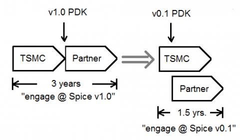
The TSMC OIP event is next week and again it is packed with a wide range of technical presentations from TSMC, top semiconductor, EDA, and IP companies, plus long time TSMC partner and ASIC provider Open-Silicon, a SiFive Company. You can see the full agenda HERE.
AI is revolutionizing and transforming virtually every industry… Read More
If you are interested in what types of chips we will see in the coming years always ask an ASIC provider because they know. Companies of all sizes (small-medium-large) use ASIC companies to get their chips out in the least amount of time and at a minimum cost because that is what ASIC companies do.
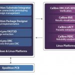
IP is an important ingredient to the … Read More
One of the more exciting design start market segments that we track is Artificial Intelligence related ASICs. With NVIDIA making billions upon billions of dollars repurposing GPUs as AI engines in the cloud, the Application Specific Integrated Circuit business was sure to follow. Google now has its Tensor Processing Unit, Intel… Read More
This year’s OIP was much more lighthearted than I remember which is understandable. TSMC is executing flawlessly, delivering new process technology every year. Last year’s opening speaker, David Keller, used the phrase “Celebrate the way we collaborate” which served as the theme for the conference. This year David’s… Read More
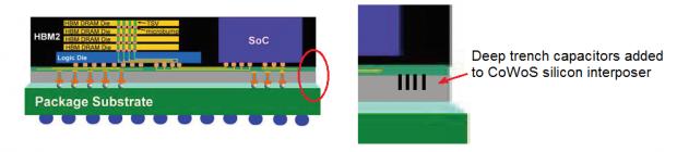
There is an emerging set of advanced packaging technologies that enables unique product designs, with the capability to integrate multiple die, from potentially heterogeneous technologies. These “system-in-package” (SiP) offerings provide architects with the opportunity to optimize product performance, power, cost,… Read More