You are currently viewing SemiWiki as a guest which gives you limited access to the site. To view blog comments and experience other SemiWiki features you must be a registered member. Registration is fast, simple, and absolutely free so please,
join our community today!
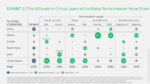
Semicap is in some ways the unsung hero of American global dominance in semiconductors. The US punches above its weight in terms of market share compared to demand, but specifically in three categories. EDA, IP, and Equipment.
I hope to write about everything there can be said about semiconductors, and EDA is a place I understand… Read More
Advanced 2.5D/3D Packaging Roadmapby Tom Dillinger on 01-03-2022 at 6:00 amCategories: Events, Semiconductor, TSMC
Frequent SemiWiki readers are no doubt familiar with the advances in packaging technology introduced over the past decade. At the recent International Electron Devices Meeting (IEDM) in San Francisco, TSMC gave an insightful presentation sharing their vision for packaging roadmap goals and challenges, to address the growing… Read More
TSMC recently held their 10th annual Open Innovation Platform (OIP) Ecosystem Forum. An earlier article summarized the highlights of the keynote presentation from L.C. Lu, TSMC Fellow and Vice-President, Design and Technology Platform, entitled “TSMC and Its Ecosystem for Innovation” (link).
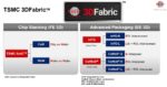
Overview of 3D Fabric
The TSMC… Read More
The recent TSMC Technology Symposium provided several announcements relative to their advanced packaging offerings.
General
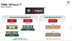
3DFabricTM
Last year, TSMC merged their 2.5D and 3D package offerings into a single, encompassing brand – 3DFabric.
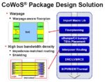
2.5D package technology – CoWoS
The 2.5D packaging options are divided into the CoWoS… Read More
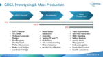
ASICs by definition are designed to meet the respective applications’ requirements. ASIC engineers deploy various design techniques to maximize performance, minimize power and reduce chip size. But is there more that can be done after the GDSII is taped out? A recent press release from Alchip Technology dated Feb 4, 2021 claims… Read More
Recently, TSMC held their 26th annual Technology Symposium, which was conducted virtually for the first time. This article is the last of three that attempts to summarize the highlights of the presentations. This article focuses on the technology design enablement roadmap, as described by Cliff Hou, SVP, R&D.
Key Takeaways… Read More
Recently, TSMC held their 26th annual Technology Symposium, which was conducted virtually for the first time. This article is the second of three that attempts to summarize the highlights of the presentations. This article focuses on the TSMC advanced packaging technology roadmap, as described by Doug Yu, VP, R&D.
Key… Read More
Summary
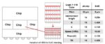
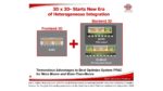
Thermo-compression bonding is used in heterogeneous 3D packaging technology – this attach method was applied to the assembly of large (12-stack and 16-stack) high bandwidth memory (HBM) die, with significant bandwidth and power improvements over traditional microbump attach.
Introduction
The rapid growth of heterogeneous… Read More
TSMC as Pure Play Wafer Foundry
TSMC started its wafer foundry business more than 30 years ago. Visionary management and creative engineering teams developed leading-edge process technologies and their reputation as trusted source for high-volume production. TSMC also recognized very early the importance of building an … Read More
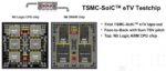
At the recent Open Innovation Platform® Ecosystem Forum in Santa Clara, TSMC provided an enlightening look into the future of heterogeneous packaging technology. Although the term chiplet packaging is often used to describe the integration of multiple silicon die of potentially widely-varying functionality, this article… Read More