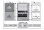
One of the most unique acronyms that I learned about this past year is ACAP from Xilinx, which stands for Adaptive Compute Acceleration Platform. At the recent Cadence LIVE event, I had the pleasure of watching Pei Yao, a Xilinx senior staff CAD engineer, as she talked about the challenges of getting all the analog and mixed-signals… Read More
Tag: 7nm
Highlights of the TSMC Technology Symposium 2021 – Silicon Technology
Recently, TSMC held their annual Technology Symposium, providing an update on the silicon process technology and packaging roadmap. This article will review the highlights of the silicon process developments and future release plans.
Subsequent articles will describe the packaging offerings and delve into technology … Read More
Is IBM’s 2nm Announcement Actually a 2nm Node?
IBM has announced the development of a 2nm process.
IBM Announcement
What was announced:
- “2nm”
- 50 billion transistors in a “thumbnail” sized area later disclosed to be 150mm2 = 333 million transistors per millimeter (MTx/mm2).
- 44nm Contacted Poly Pitch (CPP) with 12nm gate length.
- Gate All Around (GAA), there are several ways
Achronix Next-Gen FPGAs Now Shipping
Earlier in April, Achronix made a product announcement with the headline “Achronix Now Shipping Industry’s Highest Performance Speedster7t FPGA Devices.” The press release drew attention to the fact that the 7nm Speedster®7t AC7t1500 FPGAs have started shipping to customers ahead of schedule. In the complex product world… Read More
Ireland – A Model for the US on Technology
After I published a recent article about Intel, I was contacted by the Irish Development Agency (IDA) where Intel has a large fab presence and asked if I would like to interview them about the Intel site. The interview with Turlough McCormack of the IDA, started with Intel’s presence in Ireland but then went on to paint an interesting… Read More
How to Spend $100 Billion Dollars in Three Years
TSMC recently announced plans to spend $100 billion dollars over three years on capital. For 2021 they announced $30B in total capital with 80% on advanced nodes (7nm and smaller), 10% on packaging and masks and 10% on “specialty”.
If we take a guess at the capital for each year, we can project something like $30B for 2021 (announced),… Read More
SALELE Double Patterning for 7nm and 5nm Nodes
In this article, we will explore the use of self-aligned litho-etch-litho-etch (SALELE) double patterning for BEOL metal layers in the 7nm node (40 nm minimum metal pitch [1]) with DUV, and 5nm node (28 nm minimum metal pitch [2]) with EUV. First, we mention the evidence that this technique is being used; Xilinx [3] disclosed the… Read More
Intel’s IDM 2.0
In January I presented at the ISS conference a comparison of Intel’s, Samsung’s and TSMC’s leading edge offerings. You can read a write-up of my presentation here.
With the problems going on at Intel, that article generated a lot of interest in the investment community, and I have been holding a lot of calls with analysts who are trying… Read More
SPIE 2021 – ASML DUV and EUV Updates
At the SPIE Advanced Lithography Conference held in February, ASML presented the latest information on their Deep Ultraviolet (DUV) and Extreme Ultraviolet (EUV) exposure systems. I recently got to interview Mike Lercel of ASML to discuss the presentations.
DUV
Despite all the attention EUV is getting, most layers are still… Read More
Intel Node Names
There is a lot of interest right now in how Intel compares to the leading foundries and what the future may hold.
Several years ago, I published several extremely popular articles converting processes from various companies to “Equivalent Nodes” (EN). Nodes were at one time based on actual physical features of processes but had… Read More


