You are currently viewing SemiWiki as a guest which gives you limited access to the site. To view blog comments and experience other SemiWiki features you must be a registered member. Registration is fast, simple, and absolutely free so please,
join our community today!
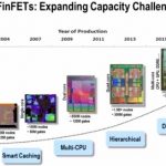
I think by now there has been good level of discussion on FinFET technology at sub-20 nm process nodes and this is an answer to ultra dense, high performance, low power, and billion+ gate SoC designs within the same area. However, it comes with some of the key challenges with respect to power, noise and reliability of the design. A FinFET… Read More
In the modern semiconductor ecosystem we are seeing rapid advancement in technology breaking past once perceived limits; 28nm, 20nm, 16-14nm, 10nm and we are foreseeing 7nm now. Double and multi-patterning are already being seen along with complex FinFET structures in transistors to gain the ultimate advantages in PPA from… Read More
There is an interesting article on Seeking Alpha about Intel. Interesting because it is written by someone with both fabless semiconductor experience and a talent for strategic thinking. It’s a good read and like most Seeking Aplha semiconductor articles the comments are hilarious. Give the guy a penny and click over HERE, he … Read More
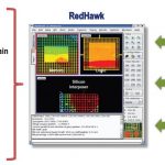
Since a few years, I have been following up Ansys Apachetools for semiconductor design, verification and sign-off. RedHawk is the most prominent platform of tools from Ansys, specifically for Power, Noise and Reliability Sign-off. It has witnessed many open endorsements from several of Ansyscustomers through open presentations,… Read More
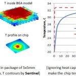
As Moore’s law started saturating on a single semiconductor die, the semiconductor community came up with the approach of growing vertically by stacking dies one above other in a 3D-IC arrangement. However, a major concern with a 3D-IC is that the heat generated by each die can get trapped in the stack, and hence it’s extremely important… Read More
At the GSA Silicon Summit this afternoon there was a discussion of 3D IC and 2.5D IC. The session was moderated by Javier DeLaCruz of eSilicon and the panelists were:
- Calvin Cheung of ASE (an OSAT)
- Gil Lvey of OptimalTest (a test house)
- Bob Patti of Tezzaron (semiconductor company specializing in TSV-based designs)
- Riko Radojcic
…
Read More
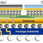
It feels to be at the top of semiconductor technology by having dies with high density of semiconductor design at sub-20nm technology node stacked together into a 3D-IC to form a complete SoC which can accommodate billions of gates. However there are multiple factors to be looked at in order to make that successful amid often conflicting… Read More
3D-IC has a stack of dies connected and packaged together, and therefore needs new testing strategies other than testing a single die. It’s given that a single defective die can render the whole of 3D-IC unusable, so each die in the stack must be completely and perfectly tested before its entry into that stack. Looking at it from a … Read More
IC designers contemplating the transition to 16nm FinFET technology for their next SoC need to be informed about design flow and IP changes, so TSMC teamed up with Cadence Design Systems today to present a webinar on that topic. I attended the webinar and will summarize my findings.
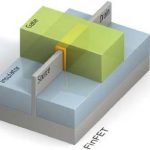
Shown below is a 3D layout concept of an ideal FinFET… Read More
At TSMC’s latest earnings call held mid January 2014, an analyst asked TSMC for a revenue forecast for their emerging 2.5/3D product line. C.C. Wei, President and Co-CEO answered: “800 Million Dollars in 2016 ”. TSMC has demonstrated great vision many times before. For me, an enthusiastic supporter of this technology, this statement… Read More