At TSMC’s latest earnings call held mid January 2014, an analyst asked TSMC for a revenue forecast for their emerging 2.5/3D product line. C.C. Wei, President and Co-CEO answered: “800 Million Dollars in 2016 ”. TSMC has demonstrated great vision many times before. For me, an enthusiastic supporter of this technology, this statement… Read More

Tag: 3d-ic
What will drive MEMS to drive I-o-T and I-o-P?

By I-o-P, I mean Internet-of-People- I couldn’t think of anything better than this to describe a technology which becomes your custodian for everything you do; you may consider it as your good companion through life or an invariably controlling spy. This is obvious with the embedded sensor techno-products such as Kolibree, a … Read More
TSMC: 3D, 450mm, CoWoS and More
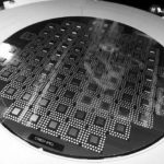
The first keynote at the Burlingame 3D conference was by Doug Yu of TSMC. Not surprisingly he was talking about 3D. In particular, TSMC has WLSI technology that they call CoWoS, which stands for chip-on-wafer-on-substrate which pretty much describes how it is built. This is the technology that Xilinx uses for its recently announced… Read More
Xilinx Pulls Back the 20nm UltraScale Curtain
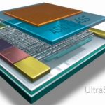
This week Xilinx has announced that “The Xilinx 20nm All Programmable UltraScale™ portfolio is now available with detailed device tables, product documentation, design tools and methodology support.”
Do you know what 20nm is? It’s small, tiny. Think about it this way, as I just learned today that one nanometer is about as long… Read More
Xilinx and TSMC: Volume Production of 3D Parts
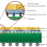
A couple of weeks ago, Xilinx and TSMC announced the production release of the Virtex-7 HT family, the industry’s first heterogeneous 3D ICs in production. With this milestone, all Xilinx 28nm 3D IC families are now in volume production. These 28nm devices were developed on TSMC’s Chip-on-Wafer-on-Substrate (CoWoS)… Read More
GlobalFoundries and ARM

GlobalFoundries had several interesting things at the ARM TechCon last week. Firstly, GlobalFoundries won the best in show award in the chip design category recognizing the best-in-class technologies introduced since the last TechCon.
Earlier in the summer GlobalFoundries and ARM announced the ARM Cortex-A12 processor,… Read More
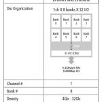
Hybrid Memory Cube Shipping
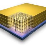
Today Micron announced that it is shipping 2GB Hybrid Memory Cube (HMC) samples. The HMC is actually 5 stacked die connected with through-silicon-vias (TSVs). The bottom die is a logic chip and is actually manufactured for Micron in an IBM 32nm process (and doesn’t have any TSVs). The other 4 die are 4Gb DRAM die manufactured… Read More
TSMC’s 16FinFET and 3D IC Reference Flows
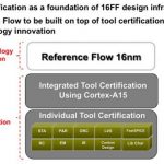
Today TSMC announced three reference flows that they have been working on along with various EDA vendors (and ARM and perhaps other IP suppliers). The three new flows are:
- 16FinFET Digital Reference Flow. Obviously this has full support for non-planar FinFET transistors including extraction, quantized pitch placement, low-vdd
Emerging Trend – Choose DRAM as per Your Design Need
Lately I was studying about new innovations in memory world such as ReRAM and Memristor. As DRAM (although it has become a commodity) has found its extensive use in mobile, PC, tablet and so on, that was an inclination too to know more about. While reviewing Cadence’s offering in memory subsystems, I came across this whitepaperwhich… Read More
What does 3D IC, FinFETs, and EUV have in common?

They are three of the top trending terms on SemiWiki and three of the hot topics at this year’s Semicon West:
In its 43rd year, SEMICON West is the flagship annual event for the global microelectronics industry. It is the premier event for the display of new products and technologies for microelectronics design and manufacturing,… Read More