You are currently viewing SemiWiki as a guest which gives you limited access to the site. To view blog comments and experience other SemiWiki features you must be a registered member. Registration is fast, simple, and absolutely free so please,
join our community today!
The 20th annual Electronic Design Process Symposium (EDPS) held April 18-19 at the Monterey Beach Hotel in Monterey California was an unqualified success. I know this because a bird (seagull?) sitting on the window sill of the conference room was so captivated by the fascinating insight provided by a number of luminaries that … Read More
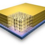
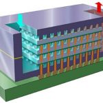
For the last few years, thru silicon via (TSV) based ICs have been looming in the mist of the future. Just how far ahead are they? Xiliinx famously has a high-end gate-array in production on a 2.5D interposer, Micron has a memory cube, TSMC has done various things in 3D that it calls CoWoS (chip on wafer on substrate), Qualcomm have been… Read More
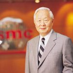
Given the compressed time between 20nm and 16nm, twelve months versus the industry average twenty four months, it is time to start talking about 10nm, absolutely. Next Tuesday is the 19th annual TSMC Technology Symposium keynoted of course by the Chairman, Dr. Morris Chang.
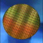
Join the 2013 TSMC Technology Symposium. Get the latest… Read More
The fabless revolution in the digital semiconductor industry is no more, with just a few integrated device manufacturers (IDMs) remaining on the playing field, it is now the normal way to do business. However, the learning curve for each new process node continues as it always has, with a host of new technical challenges for the … Read More
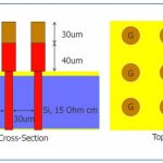
A couple of weeks ago was the 3D Architectures for Semiconductor Integration and Packagingconference in Redwood City. Cadence presented the changes that they have been making to their tool flow to enabled 2.5D (interposer-based) and true 3D TSV-based designs. You know what TSV stands for by now right? Through-silicon-via, … Read More
Late in January it is DesignCon at the Santa Clara convention center from January 28th-31st. Details are here.
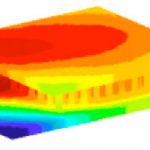
On Tuesday from 11.05 to 11.45 Apache and Ansys will be presenting on Thermal Co-analysis of 3D IC/packages/system. This is being presented by a whole team of people: Stephen Pan, senior product specialist at ANSYS; Norman… Read More
There is obviously a lot going on in 3D IC these days. And I don’t mean at the micro level of FinFETs which is also a way of going vertical. I mean through-silicon-via (TSV) based approaches for either stacking die or putting them on an interposer. Increasingly the question is no longer if this technology will be viable (there… Read More
Once upon a time (since every good story begins that way), I worked on 10kg, 70 mm diameter things that leapt out of tubes and chased after airplanes and helicopters. The electronics for these things were fairly marvelous, in the days when surface mount technology was in its infancy and having reliability problems in some situations.… Read More
At advanced process nodes, variation and its effects on the design become a huge challenge. Join Cadence® Virtuoso® experts for a series of technical webinars on variation-aware design. Learn how to use advanced technologies and tools to analyze and understand the affects of variation. We’ll introduce you to the latest Virtuoso… Read More
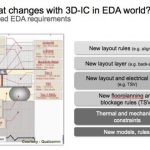
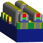
The press has been buzzing about 3D everything for the past few years, so when it comes to IC design it’s a fair question to ask how would you actually extract 3D IC structures for use by analysis tools like a circuit simulator. I read a white paper by Christen Decoin and Vassilis Kourkoulos of Mentor Graphics this week and became… Read More