

The IEEE has an Orange Country Chapter of the Components, Packaging and Manufacturing Technology Society who are organizing an all-day workshop, 3D Integrated Circuits: Technologies Enabling the Revolution. This looks to be an informative day with real-world examples in both design and test being presented by over a dozen experts. Registration details are here.
Our semiconductor industry is challenged to continually reduce product costs while simultaneously increase user features and lengthen battery life, all at a profit. 3D IC design and test is one method to satisfy these challenges.
Agenda
Welcome & Introduction
09:00 –09:05am
Opportunities and Challenges for 3D Integrated Heterogeneous Electronic Systems
09:05 –09:35am
Prof. Muhannad Bakir, Integrated 3D Systems Group, Georgia Tech, Atlanta, GA
Economics to Drive 3D Stacking
09:35 –10:05am
Dr. Phil Garrou, Microelectronic Consultants of North Carolina, Research Triangle Park, NC
Stack Silicon Interconnect Development and Key Role of Supply Chain Collaboration
10:05 –10:35am
Dr. Suresh Ramalingam, Sr. Director, Xilinx, San Jose, CA
Break
10:35 –10:45am
Emerging Challenges for Power, Signal, and Reliability Verification on 3D-IC/Silicon Interposer Designs
10:45 –11:15am
Dr. Norman Chang, Co-Founder, Apache Design Systems, Ansys, San Jose, CA
3D IC Test Challenges and Solutions
11:15AM to 11:45AM
Dr. Stephen Pateras
Product Marketing Director, Silicon to Test, Mentor Graphics
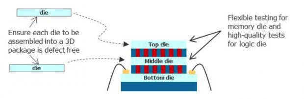
3D IC offers a compelling alternative to traditional scaling for achieving advances in performance, reduced power consumption, cost reduction, and increased functionality in a small package. Unfortunately 3D IC packaging also creates some new challenges for manufacturing test. Wafer sort will need to deliver higher test quality to ensure acceptable final package yields and thus limit the cost impact of stacking bad die in a 3D package. Stacked die also create significant test access problems since the die-level I/O may not be accessible from within the package. Ensuring that all inter-die TSV connections are adequately tested further complicates the overall test problem. This presentation will review test solutions available to cost-effectively test 3D ICs from wafer sort to packaged assembly.

Testing Challenges: higher Known Good Die (KGD), memory-on-logic configurations, logic-on-logic testing
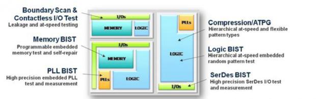
Typical SOC with an approach to testing each block
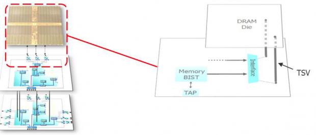
Testing a Memory die stacked on logic
Presentation Title to be announced
11:45 –12:15pm
A. La Manna, K. Rebibis, Dr. Eric Beyne, Dr. B. Swinnen, IMEC, Leuven, Belgium
Lunch
12:15 –01:15pm
Cost-Effective 3D Semiconductor Packaging Solutions Based on Embedded Die in Laminate Technology
01:15 –01:45pm
Ted Tessier, Senthil Sivaswamy, Flip Chip International LLC, Phoenix, AZ, Dr. Kazuhisa Itoi, Fujikura Ltd, Tokyo, Japan
Challenges and Solutions in Mid-end and Back-end Processes for 2.5D and 3D TSV – an OSAT Perspective
01:45 –02:15pm
Dr. YeongLee, Product and Tech. Marketing Director, STATS ChipPAC, Fremont, CA
Advanced Underfillsfor 2.5D and 3D Applications
02:15 –02:45pm
Dr. Rose Guino, Dr. Betty Huang, Dr. Kevin Becker, Dr. T. Takano, Henkel Electronic Materials, LLC, Irvine, CA
Break
02:45 –03:00pm
3D TSV Interposer and its Applications
03:00 –03:30pm
Dr. GS Kim, Founder & CEO, EPWorks, Ltd. Seoul, Korea
Via Reveal –High rate Si Thinning and Low Temperature Dielectrics for Post-TSV Processing03:30 –04:00pm
David Butler, Vice President –Marketing, SPTS Technologies, Newport, UK
Vote of Thanks
04:00 –04:05pm


TSMC CoWoS versus Intel EMIB Semiconductor Packaging