You are currently viewing SemiWiki as a guest which gives you limited access to the site. To view blog comments and experience other SemiWiki features you must be a registered member. Registration is fast, simple, and absolutely free so please,
join our community today!
I had the opportunity to preview the upcoming SemiWiki webinar titled: Design Methodologies for Next-Generation Heterogeneously Integrated 2.5/3D-IC Designs. John Park’s message, describing this powerful Cadence solution, really impressed me. That’s why I want to encourage you to register for it and join this SemiWiki … Read More
DesignCon is coming up, kicking off the first of many industry conferences for the year. It’s at the Santa Clara Convention Center which is the best venue in Northern California. Not only is this a semiconductor crowd, it’s also a systems crowd covering chips, boards, and systems. More than 175 companies participate with an expected… Read More
Dual in-line memory modules (DIMM’s ) with double data rate synchronous dynamic random access memory (DDR SDRAM) have been around since before we were worried about Y2K. Over the intervening years this format for provisioning memory has evolved from supporting DDR around 1995, to DDR1 in 2000, DDR2 in 2003, DDR4 in 2007 and DDR4… Read More
In November of 2016, I made a bold statement that October 20, 2016 would stand as a watershed day in integrated photonics. The reason for this claim was that GLOBALFOUNDRIES proclaimed that integrated photonics was real and here to stay. The same week I wrote an article about Cadence Design Systems securing a photonic beachhead … Read More
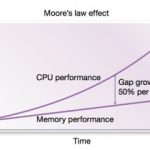
Following Moore’s Law down to 10 or even 7 nm labeled feature size demands US $ hundreds of millions of up-front investment, a very large design team and two or more years of development time. These parameters suggest that it only makes sense for very high volume applications to continue on the shrink path to increase SoCs’ functionalities.… Read More
Last week I presented at the 3D ASIP EDA Tutorial and attended the Conference. In previous years, leading edge papers were presented from large companies pushing a solution to meet their needs. These companies had the resources and clout to achieve some astounding successes, but the lingering question was: “what other product… Read More
The traditional system-on-chip (SoC) design process has fully qualified verification methods embodied in the form of process design kits (PDKs). Why is it that chip design companies and assembly houses have no IC/package co-design sign-off verification process?
Package die are often produced using multiple processes and… Read More
More news from the 3DASIP conference. Chet Palesko of SavanSys Solution had an interesting presentation with the same title as this blog (although this blog draws from several other presentations too). Chet took a look at what aspects of 3D are likely to get cheaper going forward. He took as a starting point that stuff that is not … Read More
I have been at the 3D ASIP conference that is held every year in Burlingame. It is far and away the best place to get a snapshot on what is going on in 3D (and 2.5D) IC design each year. One of the presentations was by the guys from Yole on where the industry is right now. Other presentations were on pathfinding, power reduction (did you know… Read More
3DIC in Burlingameby Paul McLellan on 12-01-2014 at 7:00 amCategories: Events
Every year in December is what I think of as the main 3D IC conference where you can get up to speed on all the latest. Officially it is called 3D Architectures for Semiconductor and Packaging or 3D ASIP. It is held in the Hyatt Regency in Burlingame (the one right by 101 near the airport). This year it is from December 10-12th.
The first… Read More