You are currently viewing SemiWiki as a guest which gives you limited access to the site. To view blog comments and experience other SemiWiki features you must be a registered member. Registration is fast, simple, and absolutely free so please,
join our community today!
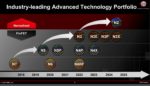
The TSMC Technical Symposium is today so I wanted to give you a brief summary of what was presented. Tom Dillinger will do a more technical review as he has done in the past. I don’t want to steal his thunder but here is what I think are the key takeaways. First a brief history lesson.
The history of TSMC Technology Development with 12 key… Read More
For the past few decades, System-on-Chip (SoC) has been the gold standard for optimizing the performance and cost of electronic systems. Pulling together practically all of a smartphone’s digital and analog capabilities into a monolithic chip, the mobile application processor serves as a near-perfect example of an SoC. But… Read More
Our smart phones, tablets, laptops and desktops are the most common consumer products with advanced 2.5D and 3D IC packaging techniques. I love seeing the product tear down articles to learn how advanced packaging techniques are being used, so at the User2User conference in Santa Clara I attended a presentation from Tarek Ramadan,… Read More
It was nice to be at a live conference again. DesignCon was held at the Santa Clara Convention Center, my favorite location, which to me there was a back to normal crowd. The sessions I attended were full and the show floor was busy. Masks and vaccinations were not required, maybe that was it. Or there was a pent-up demand to get back engaged… Read More
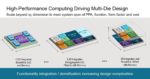
The incredible growth that the semiconductor industry has enjoyed over the last several decades is attributed to Moore’s Law. While no one argues that point, there is also industry wide acknowledgment that Moore’s Law started slowing down around the 7nm process node. While die-size reductions still scale, performance jumps… Read More
System on chip (SoC) based design has long been recognized as a powerful method to offer product differentiation through higher performance and expanded functionality. Yet, it comes with a number of limitations, such as high cost of development. Also, SoCs are monolithic, which can inhibit rapid adaptation in the face of changing… Read More
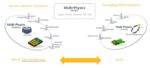
Ansys Multiphysics Platformby Tom Dillinger on 07-26-2021 at 10:00 amCategories: Ansys, Inc., EDA
Background
Traditionally, the interface between chip designers and system power, packaging, reliability, and mechanical engineering teams was a relatively straightforward exchange of specifications. Chip designers developed preliminary power dissipation estimates, often based on a simplifying power/mm**2 value. … Read More
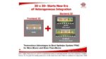
The move to true 3D IC, monolithic 3D SOC and 3D heterogeneous integration may require one of the most major design tool architecture overhauls since IC design tools were first developed. While we have been taking steps toward 3DIC with 2.5D designs with interposers, HBM, etc., the fundamental tools and flows remain intact in many… Read More
Anna has more than 25 years of expertise in managing complex R&D organizations and programs, giving birth to a number of innovative EDA technologies. She has pioneered the study and development of several generations of IC and package co-design environments and has held senior positions at leading semiconductor and EDA … Read More
TSMC as Pure Play Wafer Foundry
TSMC started its wafer foundry business more than 30 years ago. Visionary management and creative engineering teams developed leading-edge process technologies and their reputation as trusted source for high-volume production. TSMC also recognized very early the importance of building an … Read More