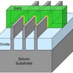
At the recent Semicon West, Michel Haond of ST Microelectronics had a presentation on 14nm FD-SOI, or what they more lengthily call UTBB FD-SOI (which when you expand it all out comes to Ultra Thin Body and Buried-Oxide Fully Depleted Silicon on Insulator). When Chenming Hu (or whoever in his group) came up with the term FinFET it … Read More
Tag: 14nm
Intel Versus TSMC 14nm Processes
Intel has begun to release some details on their 14nm process. I thought it would be interesting to contrast what Intel has disclosed to TSMC’s 16nm process disclosure from last year’s IEDM (TSMC calls their 14nm process 16nm).
[TABLE] align=”center” border=”1″
|-
| style=”width: 141px”… Read More
Who will Manufacture Apple’s Next SoC?
Just to review: The brain inside the current Apple iPhone 5s is the A7 SoC manufactured by Samsung using a 28nm process. The A6 (iPhone 5) and A5 (iPhone 4s) are based on Samsung 32nm. The rest of the Apple SoCs also used Samsung processes. I think we can all now agree that the coming Apple A8 SoC (iPhone 6) will use the TSMC 20nm process.… Read More
FD-SOI: 20nm Performance at 28nm Cost
There has been a lot of controversy about whether FD-SOI is or is not cheaper to manufacture than FinFET. Since right now FinFET is a 16nm process (22nm for Intel) and FD-SOI is, for now, a 28nm process it is not entirely clear how useful a comparison this is. Scotten Jones has very detailed process cost modeling software (that is what… Read More
The Leading Edge Foundry Landscape
There have been a lot of interesting announcements and presentations lately from the leading edge foundries. Looking at all of this information, a pretty interesting picture begins to emerge.
TSMC
TSMC is far and away the world’s largest foundry. In their 2014-Q2 conference call TSMC outlined their expectations for the balance… Read More
Samsung Foundry Explained!
Rather than watch the World Cup battle for third place, my beautiful wife and I spent last Saturday afternoon at the CASPA Wearables Symposium. The most interesting presentation was from Samsung because it included slides on their foundry offering. In regards to wearables, I still don’t see the ROI I need to buy one, yet. We are getting… Read More
Intel & Ansys Enable 14nm Chip Production
In the semiconductor industry, it feels great to hear about the process technology shrinking to lower nodes along with innovative transistor structures that offer major gains in PPA (Power, Performance and Area). However, it requires huge investment of capital, time and effort from foundries to conceptualize, prototype and… Read More
Xilinx’s 16nm vs. Altera 14nm
You will not believe this, but the family was picking me up Friday evening from the airport and on the way home… Get this, for real, the wife asks me to cut her hair tomorrow. Now the three of you that read my stuff, know what happened before. I resisted, and firmly said ‘No’…The wife seeing my macho stance began appealing to my engineer’s… Read More
Motley Fools Intel Investors Again!
It really is quite a racket. Investor bloggers spread semiconductor disinformation for $.01 per click, that coincidentally covers their stock positions, and I get paid $300 per hour to explain it to Wall Street. While I appreciate the opportunity to bond with the financial people, I do wonder how these bloggers sleep at night.… Read More
TSMC Updates: 20nm, 16nm, and 10nm!
*Spoiler Alert: The Sky is Not Falling*
The TSMC Technology Symposium last month provided a much needed technology refresh to counter aging industry experts (they make their living selling reports) who have been somewhat negative on the future of the fabless semiconductor ecosystem. If the sky wasn’t falling who would… Read More


