ASICs by definition are designed to meet the respective applications’ requirements. ASIC engineers deploy various design techniques to maximize performance, minimize power and reduce chip size. But is there more that can be done after the GDSII is taped out? A recent press release from Alchip Technology dated Feb 4, 2021 claims “High Performance Computing Demand Puts Premium on Backend Engineering Expertise.” The subheading of the same press release states “Once Mundane Service Now Prized for Squeezing Out Last nth of Performance.” From the subheading it is clear that Backend services being offered by Alchip Technology is not new. But the point that these same services have now become prized is worthwhile to understand why and how. Is it just a temporary phenomenon due to fluctuating market demand or is it a permanent shift in how the services are and will continue to be valued in the future? What are the criteria that would make one company better than another in rendering these services? The following is an attempt to arrive at answers to the above questions by taking a look at the evolution of the industry, the technologies and the supply chain ecosystem.
In the beginning semiconductor companies were vertically integrated and had their own foundries. There were dedicated departments that handled design, layout optimizations for process, packaging, test and manufacturing related aspects. With that vertical integration breaking down over the years (EDA tools, packaging, test, foundries), these capabilities needed to move out as well. Subsequently these capabilities started getting highly specialized with advances in the respective technologies.
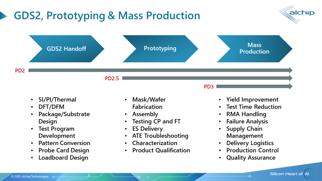
The following diagram captures what is involved in backend services. With the introduction of every new process node, packaging and substrate technologies, comes the opportunities for higher performance of the ASICs. But along with the opportunities come complexities and challenges too. The result is an increase in the outsourcing of packaging, test, assembly and production responsibilities to companies who are far more experienced in these capabilities.

To master today’s advanced manufacturing technologies and fully extract the performance, power and area benefits offered by them, specialists need to be deployed. To use an analogy from the software domain, an optimized code written in a high-level language may be further optimized at the assembly language level by an expert in that assembly language. And an optimized piece of code at the assembly language level may be further optimized at the machine code level by that machine code expert. Backend specialists are like machine code experts of the semiconductor domain.
As an example, let’s look at packaging technology. This is an area where there have been tremendous advances that directly impact the performance of a semiconductor application in terms of speed, signal and power integrity. Chip-on-Wafer-on-Substrate (CoWoS®) is one technology that enables increased performance bandwidth, reduced power consumption and smaller form factor.
Following are some excerpts from the press release.
“Packaging isn’t packaging anymore,” declares Leo Cheng, Senior Vice President of Engineering at Alchip. “With today’s design complexity, packaging has become the most cost/efficient route to increasing performance, lowering power consumption and meeting real estate constraints.
Alchip has elevated its packaging capabilities to include Chip-on-Wafer-on-Substrate (CoWoS®) first developed by TSMC and this spring is expected to announce a true 2.5D INFO capability.
Alchip’s CoWoS process runs on dedicated tooling and demonstrates IP performance equivalent to that of an original design. The process also includes online debugging and active thermal control. The company’s in-house design substrate design capabilities assure compliance with all system requirements and establishes the frame work for critical foundry-to-final test flow.
Packaging is just one of the many areas within backend services. There is value to be maximized by customers within each and every area of backend services by leveraging a specialist service provider.
Alchip with its HQ in Taipei, a dedicated team in Hsinchu and its well-honed backend services portends to bring tremendous value to its customers. It’s understandable that demand for Alchip’s post-GDSII backend services has increased exponentially across all high-performance computing ASIC applications. Any customer looking to squeeze out the last nth of performance from their semiconductor device may want to have exploratory discussions with Alchip.
Also Read:
Alchip at TSMC OIP – Reticle Size Design and Chiplet Capabilities
Alchip moves from TSMC 7nm to 5nm!
Alchip Delivers Cutting Edge Design Support for Supercomputer Processor
Share this post via:


Musk’s Orbital Compute Vision: TERAFAB and the End of the Terrestrial Data Center