Intel ushers in the next generation of AI PCs with exceptional performance, graphics and battery life; available this month.
NEWS HIGHLIGHTS:
This press release features multimedia. View the full release here: https://www.businesswire.com/news/home/20260105738564/en/
")
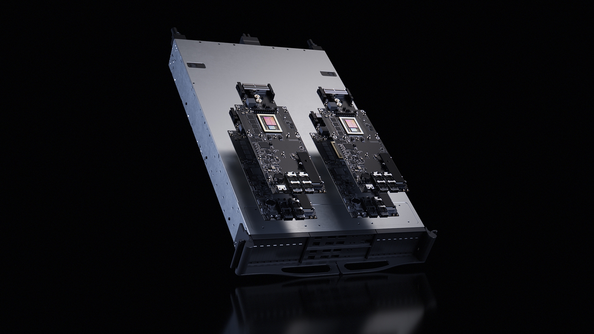
An Intel® Core™ Ultra series 3 processor. (Credit: Intel Corporation)
“With Series 3, we are laser-focused on improving power efficiency, adding more CPU performance, a bigger GPU in a class of its own, more AI compute and app compatibility you can count on with x86.” – Jim Johnson, Senior Vice President and General Manager, Client Computing Group, Intel
Series 3 Adds a New Class of Intel Core Ultra X9 and X7 Processors
Within the Intel Core Ultra Series 3 mobile lineup, a new class of Intel Core Ultra X9 and X7 processors come packed with the highest performing, integrated Intel® Arc™ graphics. They are purpose-built for multitaskers that handle advanced workloads like gaming, creation and productivity on the go. The top SKUs feature up to 16 CPU cores, 12 Xe -cores and 50 NPU TOPS, delivering up to 60% better multithread performance1, over 77% faster gaming performance2 and up to 27 hours of battery life3.
The Series 3 family also includes Intel Core processors, intentionally designed to power mainstream mobile systems. Leveraging the same foundational architecture of Intel Core Ultra Series 3, the Intel Core lineup enables more performant and efficient laptop designs at lower price points.
Series 3 Accelerates AI Adoption in Robotics, Smart Cities, Automation and Healthcare
For the first time, alongside their PC counterparts, Series 3 edge processors are certified for embedded and industrial use cases, including extended temperature ranges, deterministic performance, and 24x7 reliability.
Intel Core Ultra Series 3 delivers competitive advantages in critical edge AI workloads with up to 1.9x higher large language model (LLM) performance4, up to 2.3x better performance per watt per dollar on end-to-end video analytics5, and up to 4.5x higher throughput on vision language action (VLA) models6. The integrated AI acceleration enables superior total cost of ownership (TCO) through a single system on chip (SoC) solution versus traditional multi-chip CPU and GPU architectures.
Availability
Pre-orders for the first consumer laptops powered by Intel Core Ultra Series 3 processors will begin Jan. 6, 2026. Systems will be available globally starting Jan. 27, 2026, with additional designs coming throughout the first half of the year.
Edge systems powered by Intel Core Ultra Series 3 will be available starting Q2 2026.
About Intel
Intel (Nasdaq: INTC) designs and manufactures advanced semiconductors that connect and power the modern world. Every day, our engineers create new technologies that enhance and shape the future of computing to enable new possibilities for every customer we serve. Learn more at intel.com.
NEWS HIGHLIGHTS:
- First platform built on Intel 18A: At CES 2026, Intel launched the Intel® Core™ Ultra Series 3 processors, the first compute platform built on Intel 18A - the most advanced semiconductor process ever developed and manufactured in the United States.
- Powering over 200 PC designs: Series 3 includes a robust family of mobile processors, delivering exceptional performance, graphics and battery life.
- From PC to Edge: For the first time, Series 3 processors are tested and certified for embedded and industrial use cases at the edge like robotics, smart cities, automation, healthcare and more.
This press release features multimedia. View the full release here: https://www.businesswire.com/news/home/20260105738564/en/
An Intel® Core™ Ultra series 3 processor. (Credit: Intel Corporation)
“With Series 3, we are laser-focused on improving power efficiency, adding more CPU performance, a bigger GPU in a class of its own, more AI compute and app compatibility you can count on with x86.” – Jim Johnson, Senior Vice President and General Manager, Client Computing Group, Intel
Series 3 Adds a New Class of Intel Core Ultra X9 and X7 Processors
Within the Intel Core Ultra Series 3 mobile lineup, a new class of Intel Core Ultra X9 and X7 processors come packed with the highest performing, integrated Intel® Arc™ graphics. They are purpose-built for multitaskers that handle advanced workloads like gaming, creation and productivity on the go. The top SKUs feature up to 16 CPU cores, 12 Xe -cores and 50 NPU TOPS, delivering up to 60% better multithread performance1, over 77% faster gaming performance2 and up to 27 hours of battery life3.
The Series 3 family also includes Intel Core processors, intentionally designed to power mainstream mobile systems. Leveraging the same foundational architecture of Intel Core Ultra Series 3, the Intel Core lineup enables more performant and efficient laptop designs at lower price points.
Series 3 Accelerates AI Adoption in Robotics, Smart Cities, Automation and Healthcare
For the first time, alongside their PC counterparts, Series 3 edge processors are certified for embedded and industrial use cases, including extended temperature ranges, deterministic performance, and 24x7 reliability.
Intel Core Ultra Series 3 delivers competitive advantages in critical edge AI workloads with up to 1.9x higher large language model (LLM) performance4, up to 2.3x better performance per watt per dollar on end-to-end video analytics5, and up to 4.5x higher throughput on vision language action (VLA) models6. The integrated AI acceleration enables superior total cost of ownership (TCO) through a single system on chip (SoC) solution versus traditional multi-chip CPU and GPU architectures.
Availability
Pre-orders for the first consumer laptops powered by Intel Core Ultra Series 3 processors will begin Jan. 6, 2026. Systems will be available globally starting Jan. 27, 2026, with additional designs coming throughout the first half of the year.
Edge systems powered by Intel Core Ultra Series 3 will be available starting Q2 2026.
About Intel
Intel (Nasdaq: INTC) designs and manufactures advanced semiconductors that connect and power the modern world. Every day, our engineers create new technologies that enhance and shape the future of computing to enable new possibilities for every customer we serve. Learn more at intel.com.


")