TSMC recently held their annual Technology Symposium in Santa Clara. Part 1 of this article focused on the semiconductor process highlights. This part reviews the advanced packaging technologies presented at the symposium.
TSMC has clearly made a transition from a “pure” wafer-level foundry to a supplier of complex integrated system modules – or according to C.C. Wei, CEO, TSMC is a leading source for “nano-mass production innovations”. (Taiwan News, 4/23/19) This is the outcome of years of R&D investment – for example, see the discussion on 3D stacking in the “SoIC” section below.
Dr. Doug Yu, VP, Integrated Interconnect and Package R&D provided a detailed update. Dr. Yu classified the package technologies into unique categories – “front-end” 3D chip integration (SoIC) and “back-end” packaging advances (CoWoS, InFO). Additionally, he addressed the progress in pad pitch and Cu pillar/SnAg bump lithography, specifically mentioning the automotive grade reliability requirements.
Here’s a brief recap of the TSMC advanced packaging technology status.
Bumping
TSMC continues to advance bump technology, with 60-80um bump pitch achievable (for smaller die).
CoWoS
The initial TSMC 2.5D packaging offering was chip-on-wafer-on-substrate (CoWoS), which has enabled very high-performance system integration by bringing memory “closer to the processor”.
- >50 customer products
- TSMC is developing “standardized” configurations – e.g., 1 SoC with 2 or 4 HBMs, evolving to >2 SoCs with 8 HBM2Es (96GB @ 2.5TB/sec – wow.)
Correspondingly, TSMC will be expanding the maximum 2.5D interposer footprint from a max of 1X reticle (~50×50) to 3X (~85×85), with a 150um bump pitch.
- The silicon interposer supports 5 metal layers and a (new) deep trench capacitor – see the figure below.

InFO
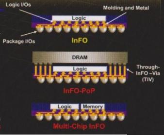
TSMC continues to evolve the Integrated FanOut (InFO) package offerings. Recall that InFO is a means of integrating (multiple) die using a “reconstituted wafer” molding compound to provide the package substrate for RDL patterning. InFO builds upon the traditional small-package WLCSP technology to enable (large area) redistribution interconnect and high bump count – see the figure below.

InFO-PoP supports stacking of a logic die and a DRAM die on top of the base, using through-InFO-vias (TIV) to connect the DRAM to the metal layers. InFO-PoP development has focused on improving the pitch and aspect ratio (vertical-to-diameter) of the TIVs.
InFO-on-Substrate offerings attach a (multi-die) InFO module to a (large area) substrate, leveraging the multiple reticle stitching technology developed for CoWoS.
SoIC (“front-end” 3D integration)
The big packaging announcement at the symposium was the introduction of the “front-end” 3D die stacking topology, denoted as SoIC (System-on-Integrated Chips).
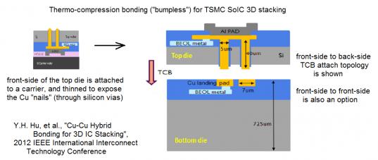
SoIC is a “bumpless” interconnect method between multiple die. As depicted in the figure below (from an early R&D paper from TSMC), Cu pads from a base die and exposed Cu “nails” from the (thinned) top die utilize thermo-compression bonding to provide the electrical connection. (An appropriate underfill material is present at the die-to-die interface, as well.)

- Through-silicon vias in the die provide connectivity, with a very tight pitch.
- Both face-to-face and face-to-back die connectivity are supported. The “known good” stacked die may be different sizes, with multiple die on a stacked layer.
- TSMC showed a mock-up of a 3-high vertical SoIC stack.
- EDA enablement is available: physical design (DRC, netlisting/LVS), parasitic extraction, timing, IR/EM analysis, signal integrity/power integrity analysis, thermal/materials stress analysis.
- The qualification target for the SoIC package offering is YE’2019. (My understanding from a separate TSMC announcement is SoIC volume availability will be in 2021.)
Dr. Yu also indicated, “The front-end SoIC module will be able to be integrated as part of a back-end 2.5D offering, as well.”
Summary
Both 2.5D and InFO “back-end” package offerings continue to evolve.
Yet, for me the highlight was the introduction of the tight-pitch, Cu compression-bonded full-3D stacked die of the SoIC topology. The available circuit density (per mm**3) will be very appealing. The challenges to leverage this technology will be considerable, though, from system architecture partitioning to complex electrical/thermal/mechanical analysis across the stacked die interfaces.
Moore’s Law is definitely alive-and-well, although it will require 3D glasses. 😀
-chipguy
Also read: 2019 TSMC Technology Symposium Review Part I
Share this post via:


Comments
6 Replies to “TSMC Technology Symposium Review Part II”
You must register or log in to view/post comments.