The recent TSMC Technology Symposium provided several announcements relative to their advanced packaging offerings.
General
3DFabricTM
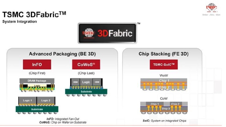
Last year, TSMC merged their 2.5D and 3D package offerings into a single, encompassing brand – 3DFabric.
2.5D package technology – CoWoS
The 2.5D packaging options are divided into the CoWoS and InFO families.
- CoWoS-S
The “traditional” chip-on-wafer-on-substrate with silicon interposer for die-to-die redistribution layer (RDL) connectivity is celebrating its 10th year of high-volume manufacturing.
- CoWoS-R
The CoWoS-R option replaces the (expensive) silicon interposer spanning the extent of the 2.5D die placement area with an organic substrate interposer. The tradeoff for the CoWoS-R is the less aggressive line pitch for the RDL interconnects – e.g., 4um pitch on the organic, compared to sub-um pitch for CoWoS-S.
- CoWoS-L
Between the silicon –S and organic –R interposer options, the TSMC CoWoS family includes a newer addition, with a “local” silicon bridge for (ultra-short reach) interconnect between adjacent die edges. These silicon slivers are embedded in an organic substrate, providing both high density USR connections (with tight L/S pitch) and the interconnection and power distribution features of (thick) wires and planes on an organic substrate.
Note that CoWoS is designated as a “chip last” assembly flow, with die attached to the fabricated interposer.
- 2.5D package technology – InFO
InFO utilizes (single or multiple) die on a carrier that are subsequently embedded in a reconstituted wafer of molding compound. The RDL interconnect and dielectric layers are subsequently fabricated on the wafer, a “chip-first” process flow. The single-die InFO provides a high-bump count option, with the RDL wires extending outward from the die area – i.e., a “fan-out” topology. As illustrated below, the multi-die InFO technology options include:
-
- InFO-PoP: “package-on-package”
- InFO-oS: “InFO assembly-on-substrate”

- 3D packaging technology – SoIC
The 3D packages are associated with the SoIC platform, which utilizes stacked die with direct pad bonding, in either face-to-face or face-to-back orientations – denoted as SoIC chip-on-wafer. Through silicon vias (TSVs) provide connectivity through a die in the 3D stack.
The SoIC development roadmap is illustrated below – as an example, N7-on-N7 die configurations will be qualified in 4Q21.

New Packaging Technology Announcements
There were several key announcements at this year’s Symposium.
- maximum package size and RDL enhancements
The demand for a larger number of 2.5D die integrated into a single package drives the need for RDL fabrication across a larger area, whether on an interposer or the reconstituted wafer. TSMC has continued to extend the “stitching” of interconnects past the single exposure maximum reticle size. Similarly, there is a need for additional RDL layers (with aggressive wire pitch).
The roadmap for larger package sizes and RDL layers includes:
-
- CoWoS-S: 3X reticle (qualified by YE’2021)
- CoWoS-R: 45X reticle (3X in 2022), 4 RDL layers on the organic substrate (W/S: 2um/2um), in reliability qualification using an SoC + 2 HBM2 die stacks
- CoWoS-L: test vehicle in reliability assessment at 1.5X reticle size, with 4 local interconnect bridges between 1 SoC and 4 HBM2 die stacks
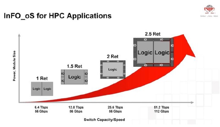
- InFO_oS: 5X reticle (51mm x 42mm, on a 110mm x 110mm package), 5 RDL layers (W/S: 2um/2um), currently in reliability assessment
The figure below illustrates a potential InFO_oS configuration, with logic die surrounded by I/O SerDes chiplets, in support of a high-speed/high-radix network switch.
-
- InFO_B (bottom)
The InFO_PoP configuration shown above depicts an InFO assembly with a DRAM module attached on top, with vias between the DRAM and the RDL interconnect layers.
TSMC is altering this InFO_PoP offering, to enable the (LPDDR DRAM) package assembly to be completed at an external contract manufacturer/OSAT, an option denoted at InFO_B, as shown below.

Correspondingly, TSMC has extended the “Open Innovation Platform” to include 3DFabric partners qualified for InFO_B final assembly. (Currently, the 3DFabric partner companies are: Amkor Technology, ASE Group, Integrated Service Technology, and SK Hynix.)
-
- CoWoS-S “standard architecture” (STAR)
A prevalent design implementation for CoWoS-S is the integration of a single SoC with multiple High-Bandwidth Memory (HBM) die stacks. The data bus width between the logic die and the HBM2E (2nd generation) stacks is very large – i.e., 1024 bits.
The routing and signal integrity challenges to connect the HBM stacks to the SoC through the RDL are considerable. TSMC is providing systems companies with several standard CoWoS-S design configurations to expedite engineering development and electrical analysis schedules. The figure below illustrates some of the different CoWoS-S options, ranging from 2 to 6 HBM2E stacks.
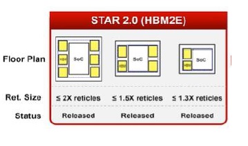
TSMC anticipates a high adoption rate of these standard design implementations in 2021.
- new TIM materials
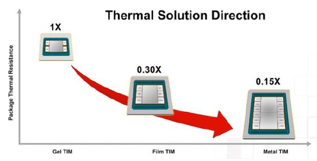
A thermal interface material (TIM) thin film is commonly incorporated into an advanced package, to help reduce the total thermal resistance from the active die to the ambient environment. (For very high power devices, there are commonly two TIM material layers applied – an internal layer between the die and package lid and one between the package and heat sink.)
Corresponding to the increased power dissipation of larger package configurations, the TSMC advanced packaging R&D team is pursuing new internal TIM material options, as depicted below.
- advanced packaging (AP) manufacturing capacity expansion
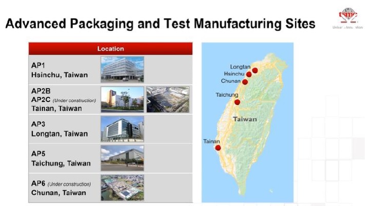
In anticipation of increased adoption of the full complement of 3DFabric packaging, TSMC is investing significantly in expanding the advanced packaging (AP) manufacturing capacity, as illustrated below.
For more information on TSMC’s 3DFabric technology, please follow this link.
-chipguy
Share this post via:


Comments
2 Replies to “Highlights of the TSMC Technology Symposium 2021 – Packaging”
You must register or log in to view/post comments.