Recently, TSMC held their 26th annual Technology Symposium, which was conducted virtually for the first time. This article is the second of three that attempts to summarize the highlights of the presentations. This article focuses on the TSMC advanced packaging technology roadmap, as described by Doug Yu, VP, R&D.
Key Takeaways
- SoIC (3D) multi-die integration will benefit from continuous process improvement on die bond pitch, driven by the areal density scaling of N7, N5, and N3.
- The “back-end, die-first” InFO (2.5D) technology is being enhanced to embed a Local Silicon Interconnect (LSI) bridge, denoted as InFO-L.
- The “back-end, die-last” CoWoS (2.5D) technology is also expanded to include a LSI bridge, embedded in an organic substrate (replacing the traditional silicon interposer). CoWoS-L will offer a cost-effective method to integrate multiple die with memory stacks.
- InFO offerings are being enhanced to support larger assemblies, with RDL interconnects spanning >1X max reticle size. Similarly, CoWoS interposer dimensions will support >>1X max reticle size.
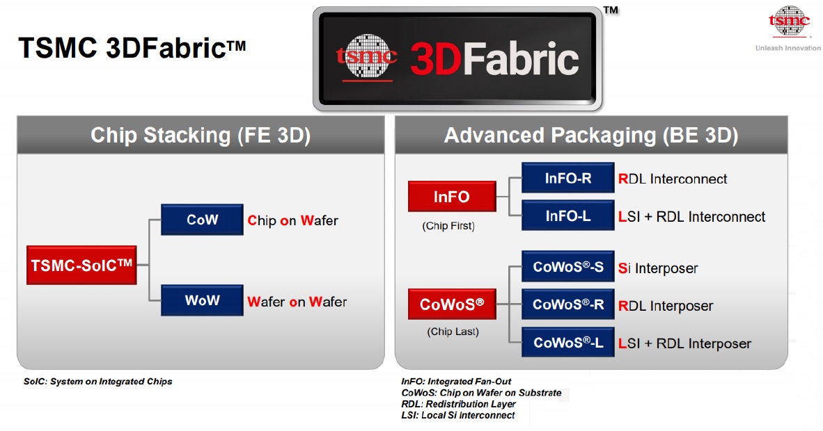
- The full complement of SoIC, InFO, and CoWoS offerings have been incorporated into the TSMC “3D Fabric” product family, in anticipation of future system-level assemblies integrating both the 3D and 2.5D packaging technologies.
Introduction
Doug’s presentation covered the pillars of TSMC’s advanced packaging options:
- the “front-end” SOIC die-to-die attach technology
- the “back-end, chip-first” InFO (Integrated FanOut) technology
- the “back-end, chip-last” CoWoS (Chip-on-Wafer-on-Substrate) technology
As will be discussed shortly, Doug announced several unique enhancements to the back-end options.
TSMC has grouped both the front-end and back-end options into a single package development roadmap, denoted as “3D Fabric”. The last section of this article will illustrate how both these FE and BE technologies can be combined, into a complex 3D package solution.
SoIC
Background
SoIC technology enables direct die-to-die attach, using thermo-compression bonding between pads – here’s an earlier article that describes this process: link.
Both face-to-face and face-to-back orientations are supported. The face-to-back topology utilizes through silicon vias (TSVs) to provide the bonding pads. TSVs also enable the addition of microbumps for subsequent package substrate attach.
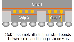
(There is a variant of this technology that enables a highly efficient assembly flow, in the specific case where both die share the same footprint – “WoW’, for Wafer-on-Wafer.)
There are opportunities for integrating multiple die at the same level to the underlying base die (as in the figure above), as well as the capability to develop a vertical stack of thinned die. The latter configuration is commonly used to construct high-bandwidth memory (HBM) stacks, with several memory die on top of a memory controller as the base. Doug referenced a recently TSMC technical presentation illustrating a 12-high HBM stack (total thickness ~60um), utilizing the SoIC bonding technology. (Reference: Tsai, C.H., et al., “Low Temperature SoIC Bonding and Stacking Technology for 12/16-Hi High Bandwidth Memory (HBM)”, VLSI 2020 Symposium, Paper TH1.1.)

Advanced SoIC Development
- thermal R (Tr)
An area of focus for SoIC development is the thermal resistance of the bond connections – it is critical that the heat generated within the die stack have a low Tr path to the package. Doug’s presentation highlighted the continuous process improvement (CPI) activity that has reduced the bond Tr by ~25%. (Similar CPI attention has been placed on reducing the Tr for microbump connections as well, by ~18%.)
- bond pitch
Another major focus area is to scale the SoIC bond and TSV pitches, in conjunction with the areal density scaling of successive process nodes. (If the bond and TSV pitch didn’t scale, that would adversely impact the realized density gains from migrating to the next node.) Doug indicated the minimum bond and TSV pitches will indeed transition from 9um (N7) to 6um (N5) and to 4.5um (N3). Doug also shared experimental data illustrating sub-um bond pitch reliability, for future node scaling.
Clearly, front-end SoIC packaging technology development is receiving considerable R&D investment.
InFO
Background
The Integrated FanOut technology utilizes a “back-end, chip-first” package assembly process. As described in the earlier article mentioned above, InFO selects known good die and encapsulates them in a “reconstituted” wafer of an epoxy molding compound.
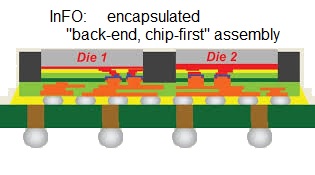
This enables the addition and patterning of dielectric and interconnect layers on top of the molding compound wafer to utilize existing fab equipment. These interconnects, along with the final pattern of metal to the package attach microbumps, are collectively described as the redistribution layers (RDL).
As will be described shortly, TSMC is introducing alternative InFO technologies – the traditional InFO assembly with redistribution layers is now denoted as InFO-R.
There are other existing InFO designations – e.g., InFO-AIP with “antenna-in-package”, and InFO-PoP with “package-on-package”. InFO-PoP integrates a chip stacked on top of the InFO assembly, whose microbumps attach to through-InFO vias (TIVs) in the molding compound to the RDL layers – see below.

The focus of the InFO package development presented at the Symposium was on enhancements to InFO-R, and a new InFO topology.
InFO-R Development
- increasing reticle size
To enable greater flexibility in multi-die integration, TSMC has begun offering InFO assembly – e.g., die placement, encapsulation, and (specifically) RDL patterning – that exceeds the maximum photolithography reticle size. The CoWoS technology has offered interconnect patterning on the silicon interposer that exceeds the 1X reticle size limit for some time; this technique has recently been extended to InFO. (1X maximum reticle size: ~33mm x 26mm.)
Support for an InFO 1.7X reticle-size assembly will be available in 4Q20, with 2.5X in 1Q21 (qualified on a final package of 110mm x 110mm). It is evident that there is significant customer demand for a low-cost package technology for ever-increasing multi-die configurations.
- RDL interconnect
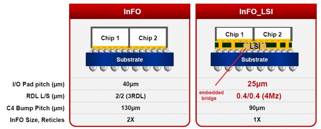
Key parameters for InFO-R are: the die pad pitch to the RDL layers (40um), the RDL pitch (2um L/2um S), and the number of RDL layers (3).
Recently, TSMC R&D published an article describing development of sub-micron L/S patterning – more die in a large InFO-R assembly will require greater interconnect routing density. (Reference: Pu, et al., IEEE ECTC, 2018, p. 45-51.)
InFO-L
As mentioned above, the RDL line/space pitch is a key characteristics of the multi-die InFO assembly. Yet, this dimension is limited by the processes available for the deposition, patterning, and curing of the organic dielectric and metallization used for the RDL layers.
To enable greater die-to-die routing capacity, TSMC is introducing a Local Silicon Interconnect (LSI) “bridge chiplet” embedded within the RDL assembly on top of the encapsulated die. Compared to the baseline InFO-R technology, the embedded silicon bridge in InFO-L offers:
- 25 um die pad pitch for LSI connectivity (versus 40um)
- 0.4um/0.4um L/S (versus 2um/2um)
- 4 metal layers (using TSMC’s “Mz” metal thickness process module)
- InFO-L will be qualified in 1Q21, on a 1X reticle-size assembly
InFO-SoIS
The typical package substrate used with InFO-R provides connectivity from the InFO bumps to the package BGA balls, with limited interconnect layers within the substrate. At the Symposium, TSMC shoed a unique variant of InFO-R, where the substrate consists of a composite of organic layers, providing 14 metal interconnect planes. This demonstration of a “System-on-Integrated Substrate” may evolve to production status for a large-area, multi-die InFO-R assembly requiring more connectivity to BGA balls.

CoWoS
Background
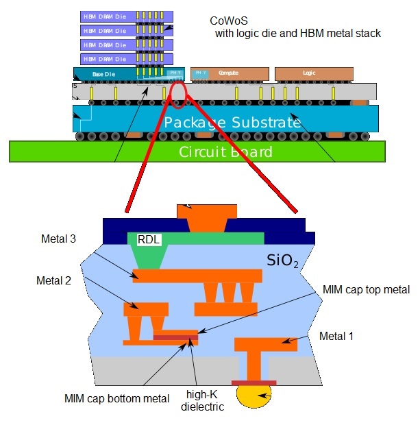
The back-end, chip-last assembly known as Chip-on-Wafer-on-Substrate (CoWoS) technology has traditionally used a silicon interposer as the intermediate-level interconnect substrate for multi-die integration. This option has been the mainstay for system implementations with an array of processor die, typically with multiple HBM memory stacks.
- reticle size
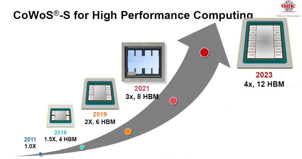
Over the years, CoWoS technology development has focused on supporting increasing silicon interposer dimensions. TSMC will be expanding the interposer size to 3X max reticle (2021) and 4X max reticle (2023), to support model processors and HBM stacks in the overall package.
- improved interposer electrical characteristics
CoWoS process R&D has enabled the following enhancements:
– up to 5 Cu metal layers
– lower sheet resistivity (improving by 3X in 1H21)
– embedded capacitors
The traditional CoWoS topology with silicon interposer is now designated as CoWoS-S, to differentiate from the new configurations that Doug presented at the Symposium.
CoWoS-L
A new chip-last offering was introduced – CoWoS-L. Like the embedded LSI interconnect bridge added to the InFO offering, a similar configuration is being added to the CoWoS assembly. The silicon interposer is replaced by an organic substrate with an embedded LSI chiplet, offering interposer-like interconnect signal density in a more cost-effective assembly.
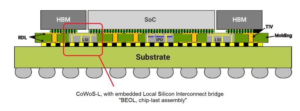
CoWoS-L plans are to provide: 1.5X reticle size (1 die, 4 HBM2E stacks), currently in production; 3X reticle size (3 die, 8 HBM2E stacks), in 2Q21.
Full Front-End (3D) and Back-End (2.5D) Integration
The 3D Fabric product initiative envisions a combination of (SoIC + InFO) and (SoIC + CoWoS) assemblies. A multi-die, multi-tiered SoIC could be integrated as part of a (chip-first) encapsulated InFO offering. An example is illustrated below of an SoIC integrated as part of a (chip-last) CoWoS assembly.

The full 3D Fabric offering is illustrated below.

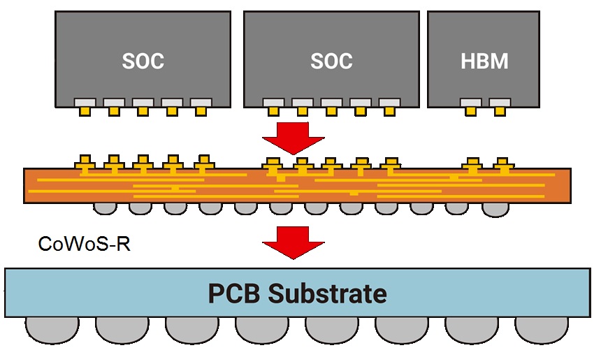
In the 3D Fabric collection, note that there is also a CoWoS-R variant shown – a chip-last assembly on an organic substrate with RDL layers and no embedded LSI bridge. Given the large number of wires required in the typical CoWoS die plus HBM stack topology, the embedded LSI bridge of CoWoS-L is likely required. Here’s a cross-section of CoWoS-R.
TSMC has made a major investment in advanced packaging development – SoIC, InFO, and CoWoS have become an integral part of system architecture definition. Increasingly, architects will need enhanced “pathfinding” tools to assist with the myriad of performance, power, area/volume, signal integrity, power delivery, thermal dissipation, reliability, and cost tradeoffs.
For more info on the full suite of 3D Fabric offerings, please follow this link.
-chipguy
Highlights of the TSMC Technology Symposium – Part 1
Highlights of the TSMC Technology Symposium – Part 3
Share this post via:


Comments
There are no comments yet.
You must register or log in to view/post comments.