Summary
The growing significance of ultra-short reach (USR) interfaces on 2.5D packaging technology has led to a variety of electrical definitions and circuit implementations. TSMC recently presented the approach adopted by their IP development team, for a parallel-bus, clock-forwarded USR interface to optimize power/performance/area – i.e., “LIPINCON”.
Introduction
The recent advances in heterogeneous, multi-die 2.5D packaging technology have resulted in a new class of interfaces – i.e., ultra-short reach (USR) – whose electrical characteristics differ greatly from traditional printed circuit board traces. Whereas the serial communications lane of SerDes IP is required for long, lossy connections, the short-reach interfaces support a parallel bus architecture.
The SerDes signal requires (50 ohm) termination to minimize reflections and reduce far-end crosstalk, adding to the power dissipation. The electrically-short interfaces within the 2.5D package do not require termination. Rather than “recovering” the clock embedded within the serial data stream, with the associated clock-data recovery (CDR) circuit area and power, these parallel interfaces can use a simpler “clock-forwarded” circuit design – a transmitted clock signal is provided with a group of N data signals.
Another advantage of this interface is that the circuit design requirements for electrostatic discharge protection (ESD) between die are much reduced. Internal package connections will have lower ESD voltage stress constraints, saving considerable I/O circuit area (and significantly reducing I/O parasitics).
The unique interface design requirements between die in a 2.5D package has led to the use of the term “chiplet”, as the full-chip design overhead of SerDes links is not required. Yet, to date, there have been quite varied circuit and physical implementation approaches used for these USR interfaces.
TSMC’s LIPINCON interface definition
At an invited talk for the recent VLSI 2020 Symposium, TSMC presented their proposal for a parallel-bus, clock-forwarded architecture – “LIPINCON” – which is short for “low-voltage, in-package interconnect”. [1] This article briefly reviews the highlights of that presentation.
The key parameters of the short-reach interface design are:
- Data rate per pin: dependent upon trace length/insertion loss, power dissipation, required circuit timing margins
- Bus width: with modularity to define sub-channels
- Energy efficiency: measured in pJ/bit, including not only the I/O driver/receiver circuits, but any additional data pre-fetch/queuing and/or encoding/decoding logic
- “Beachfront” (linear) and area efficiencies: measure of the aggregate data bandwidth per linear edge and area perimeter on the chiplets – i.e., Tbps/mm and Tbps/mm**2; dependent upon the signal bump pitch, and the number and pitch of the metal redistribution layers on the 2.5D substrate, which defines the number of bump rows for which signal traces can be routed – see the figures below
- Latency: another performance metric; the time between the initiation of data transmit and receive, measured in “unit intervals” of the transmit cycle
Architects are seeking to maximize the aggregate data bandwidth (bus width * data rate), while achieving very low dissipated energy per bit. These key design measures apply whether the chiplet interface is between multiple processors (or SoCs), processor-to-memory, or processor-to-I/O controller functionality.


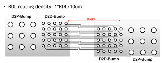
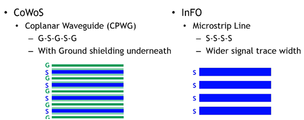
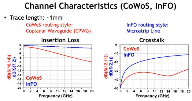
The physical signal implementation will differ, depending on the packaging technology. The signal redistribution layers (RDL) for a 2.5D package with silicon interposer will leverage the finer metal pitch available (e.g., TSMC’s CoWoS). For a multi-die package utilizing the reconstituted wafer substrate to embed the die, the RDL layers are much thicker, with a wider pitch (e.g., TSMC’s InFO). The figures below illustrate the typical signal trace shielding (and lack of shielding) associated with CoWoS and InFO designs, and the corresponding signal insertion and far-end crosstalk loss.
The key characteristics of the TSMC LIPINCON IP definition are illustrated schematically in the figure below.
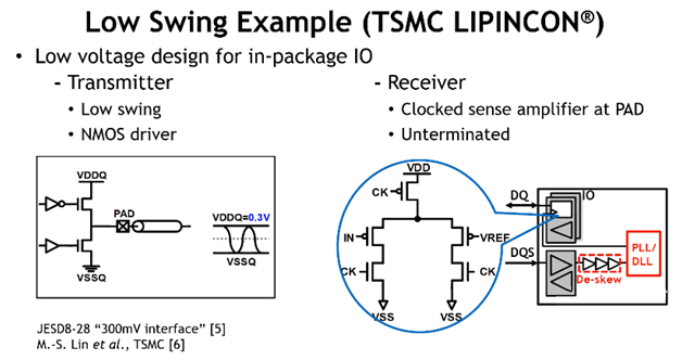
- A low signal swing interface of 0.3V is adopted (also saves power).
- The data receiver uses a simple differential circuit, with a reference input to set the switching threshold (e.g., 150mV).
- A clock/strobe signal is forwarded with (a sub-channel of) data signals; the receiver utilizes a simple delay-locked loop (DLL) to “lock” to this clock.
Briefly, a DLL is a unique circuit – it consists of an (even-numbered) chain of identical delay cells. The figure below illustrates an example of the delay chain. [2] The switching delay of each stage is dynamically adjusted by modulating the voltage inputs to the series nFET and pFET devices in the input inverter of each stage – i.e., a “current-starved” inverter. (Other delay chain implementations dynamically modify the identical capacitive load at each stage output, rather than adjusting the internal transistor drive strength of each stage.)

The “loop” in the DLL is formed by a phase detector (XOR-type logic with low-pass filter), which compares the input clock to the final output of the chain. The leading or lagging nature of the input clock relative to the chain output adjusts the inverter control voltages – thus, the overall delay of the chain is “locked” to the input clock. The (equal) delays of each stage in the DLL chain provides outputs that correspond to a specific phase of the input clock signal. The parallel data is captured in receiver flops using an appropriate phase output, a means of compensating for any data-to-clock skew across the interface.
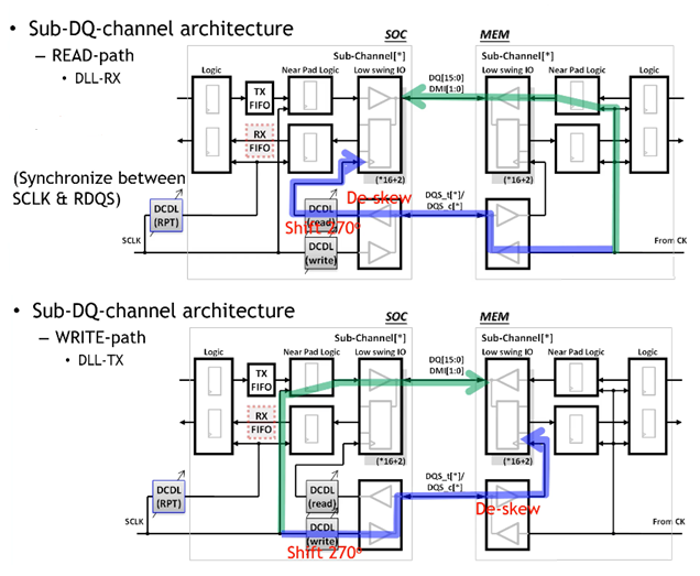
The TSMC IP team developed an innovative approach for the specific case of a SoC-to-memory interface. The memory chiplet may not necessarily embed a DLL to capture signal inputs. For a very wide interface – e.g., 512 addresses, 256 data bits, divided into sub-channels – the overhead of the DLL circuitry in the cost-sensitive memory chiplet would be high. As illustrated in the figure below, the DLL phase output which serves as the input strobe for a memory write cycle is present in the SoC instead. (The memory read path is also illustrated in the figure, illustrating how the data strobe from the memory is connected to the read_DLL circuit input.)
For the parallel LIPINCON interface, simultaneous switch noise (SSN) related to signal crosstalk is a concern. For the shielded (CoWoS) and unshielded (InFO) RDL signal connections illustrated above, TSMC presented results illustrating very manageable crosstalk for this low-swing signaling.
To be sure, designers would have the option of developing a logical interface between chiplets that used data encoding to minimize signal transition activity in successive cycles. The simplest method would be to add data bus inversion (DBI) coding – the data in the next cycle could be compared to the current data, and transmitted using true or inverted values to minimize the switching activity. An additional DBI signal between chiplets carries this decision for the receiver to decode the values.
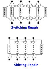
The development of heterogeneous 2.5D packaging relies upon the integration of known good die/chiplets (KGD). Nevertheless, the post-assembly yield of the final package can be enhanced by the addition of redundant lanes which can be selected after package test (ideally, built-in self-test). The TSMC presentation included examples of redundant lane topologies which could be incorporated into the chiplet designs. The figure below illustrates a couple of architectures for inserting redundant through-silicon-vias (TSVs) into the interconnections. This would be a package yield versus circuit overhead tradeoff when architecting the interface between chiplets.
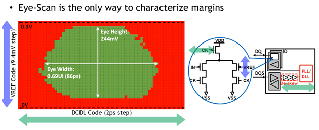
In a SerDes-based design, thorough circuit and PCB interconnect extraction plus simulation is used to analyze the signal losses. The variations in signal jitter and magnitude are analyzed against the receiver sense amp voltage differential. Hardware lab-based probing is also undertaken to ensure a suitable “eye opening” for data capture at the receiver. TSMC highlighted that this type of interface validation is not feasible with the 2.5D package technology. As illustrated below, a novel method was developed by their IP team to introduce variation into the LIPINCON transmit driver and receive capture circuitry to create an equivalent eye diagram for hardware validation.
The TSMC presentation mentioned that some of their customers have developed their own IP implementations for USR interface design. One example showed a very low swing (0.2V) electrical definition that is “ground referenced” (e.g., signal swings above and below ground). Yet, for fabless customers seeking to leverage advanced packaging, without the design resources to “roll their own” chiplet interface circuitry, the TSMC LIPINCON IP definition is an extremely attractive alternative. And, frankly, given the momentum that TSMC is able to provide, this definition will likely help accelerate a “standard” electrical definition among developers seeking to capture IP and chiplet design market opportunities.
For more information on TSMC’s LIPINCON definition, please follow this link.
-chipguy
References
[1] Hsieh, Kenny C.H., “Chiplet-to-Chiplet Communication Circuits for 2.5D/3D Integration Technologies”, VLSI 2020 Symposium, Paper SC2.6 (invited short course).
[2] Jovanovic, G., et al., “Delay Locked Loop with Linear Delay Element”, International Conference on Telecommunication, 2005, https://ieeexplore.ieee.org/document/1572136
Images supplied by the VLSI Symposium on Technology & Circuits 2020.
Share this post via:


Comments
There are no comments yet.
You must register or log in to view/post comments.