You are currently viewing SemiWiki as a guest which gives you limited access to the site. To view blog comments and experience other SemiWiki features you must be a registered member. Registration is fast, simple, and absolutely free so please, join our community today!
In December 2023, we published the Intel Revenue forecast for external wafer sales, gave a breakdown on how customers plan to ramp the foundry. The forecast is still valid (it assumes Intel executes on all plans) but since then we have a better understanding of Intel’s strategy and scenarios that could unfold.
The scenarios are based on Intel’s strengths and weaknesses which are quite different than TSMC and quite different than what we expected 2-3 years ago.
Background:
In 2019-2021, it became clear that Intel was a distant follower to TSMC in technology and that they needed to catch up or just outsource everything to TSMC/Samsung/others. Intel BUs complained about technology delay and cost and wanted to work with TSMC.
• It seemed like Intel would move to outsource, but Pat changed the plans based on discussions in 2021. Intel would allow BUs to choose Internal or TSMC. They would (and still do) come up with dual sourcing options and plans until later in the product development lifecycle.
• Intel cannot lead in tech with the small scale of current Intel (Times change, Intel is the third priority for equipment companies). Equipment vendors do much of the process and all of the tool development. You need scale to get their support. So Intel needs to offer foundry services to roughly double the scale of Intel wafer output. Intel needed to go “all in” on being a leading foundry.
• Pat [hypothetically] said: “…Business units say manufacturing is the problem. Manufacturing say BU is the problem. Fine …. Each of you can do what you want…. BUT we will make major decisions based on your execution.”
Hence where we are today: Intel is ramping TSMC on chips for processors of all types. Some leading products are 100% TSMC. And Intel is promoting foundry for others at the same time. 5 nodes in 4 years (not really, but that is a different report).
The BUs are extremely happy with this. So far multiple products have been moved to TSMC and the flexibility in using N5,N3,N2 is something they love. TSMC price is about the same as Intel’s cost, so BU margins will increase.
But how does Intel compete cost effectively with TSMC and ramp foundry and pay for all these fabs?
We overlooked a couple things until our IEDM discussions with various people in December 2023.
• Intel still wants to win and be better than TSMC. It seems unlikely… but it might not matter.
• The US government buys chips for internal products and DoD items. No strategic DoD product has TSMC parts in it. TSMC does not meet the criteria. As a result, those products have technologies that are not close to leading edge. IBM (past), GF and other defense approved companies make chips for those products but they are nowhere near leading edge. They would love to use leading edge but they need a DoD approved US company. While DoD parts are relatively low volume, the government could expand this to any Government supply chain (they track detailed supply chain and factories for all parts). IRS, Social Security, etc. TSMC cannot fill this today and it would require massive regulation to even have Samsung US or TSMC US support it. Trust me, I have done the audits with government products before, it can be extremely painful.
Also, While Intel is not set up from a scale or from a cultural perspective to be a leader in cost, US Government pays cost plus and incredibly high prices for products. Intel could have half filled fabs and still have great margins. You can see this at some government suppliers today.
• The third one also could have been predicted but was missed. Leading edge is too expensive and complex. So many foundries…. GF, UMC, SMIC, Grace, Tower have no ability to provide leading edge or even 2 generations behind technology. Intel can partner with them, provide “more modern” technologies, provide scale etc. All companies not named TSMC or Samsung could GREATLY benefit from partnering with Intel and this allows them to compete with Samsung and TSMC.
Based on the above strategies. Intel could outsource most of its silicon to TSMC to keep the BUs happy and STILL be a leader in foundry just based on being the “US Fab company” and “advanced fabs to other foundries”. These customers are much more compatible with Intel than selling to Apple, AMD, Nvidia, and Broadcom.
This is a different foundry model but one where Intel has a strength and can potentially dominate. This all may or may not work. We have quantitative milestones you can track to see if Intel is successful.
The Three Potential Foundry Scenarios are:
• *Intel Foundry Success*: Intel has competitive processes at competitive prices and ramps up to be another dominant leading edge foundry. Intel is leader and Intel BUs use Intel processes. Revenue and profits grow.
• *Intel fills TSMC gaps*: Intel supplies all other foundries, Intel supplies government. Both have few other options so they pay the price needed. Revenue grows steadily over then next 10-15 years.
• *Intel is IDM2.0 = IBM2.0*: Intel struggles to ramp government work and factories. Intel’s foundry partners decide it’s not worth it to work with them and the processes are unsuccessful. The fabs are given away, or cancelled, or underloaded. Eventually Intel foundry is absorbed.
We have more details on each and in the next few years, the probability of each scenario will change. We have updates on the probability and what tactics, models, and strategies Intel is using. More importantly we provide milestones so others can track progress…. and we track the impact to P&L and Capex.
Foundry Day Update (BREAKING NEWS): All of the presentations and commitments support the background we show, the strategies, and the scenarios.
For the 2024 SEMI International Strategy Symposium I was challenged by members of the organizing committee to look at where logic will be in ten years from a technology, economics, and sustainability perspective. The following is a discussion of my presentation.
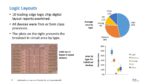
To understand logic, I believe it is useful to understand what makes up leading edge logic devices. TechInsights produces detail footprint analysis reports, and I took reports for ten 7nm and 5nm class devices including Intel and AMD microprocessors, Apple A series and M series processors, an NVIDIA GPU, and other devices. Figure 1 illustrates what makes up the die area.
Figure 1. Logic Layouts
From figure 1 logic makes up slightly less than one half of the die area, memory slightly less that one third of the die and I/O, analog, and other the balance. I find it interesting that the SRAM memory areas actually measured is a lot smaller than the percentage I typically hear people talk about for System On a Chip (SOC) products. The plot on the bottom right shows that there is one outlier but otherwise the values are tightly clustered.
Singe logic makes up almost half the die area, it makes sense to start with the logic part of the design. Logic designs are done with standard cells and figure 2 is a plan view of a standard cell.
Figure 2. Standard Cells
The height of a standard cell is typically characterized as the Metal 2 Pitch (M2P) multiplied by the number of tracks, but looking at the right side of the figure there is a cross sectional view of the device structure that must also match the cell height and is constrained by device physics. The same is the case for the cell width that depends on the Contacted Poly Pitch (CPP) and looking at the bottom of the figure there is a cross sectional view of the device structure that once again is constrained by physics.
Figure 3 presents the result of an analysis to determine the practical limits of cell width and cell height scaling. I have a presentation that details the scaling constraints and in that presentation there are dozens of slides between figure 2 and figure 3, but with limited time I could only show the conclusion.
Figure 3. Logic Cell Scaling
Cell width scaling depends on CPP, and the left side of the figure illustrates how CPP is made up of Gate Length (Lg), Contact Width (Wc) and two Contact to Gate Spacer Thicknesses (Tsp). Lg is constrained by leakage and the minimum Lg with acceptable leakage depends on the device type. Planar devices with a single gate controlling the surface of a channel with an unconstrained thickness, is limited to approximately 30nm. FinFETs and horizontal Nanosheets (HNS) constrain the channel thickness (~5nm) and have 3 and 4 gates respectively. Finally, 2D materials introduce <1nm channel thickness, non silicon materials and can produce Lg down to ~5nm. Both Wc and Tsp have limited ability to scale due to parasitics, The bottom line is a 2D device can likely produce a ~30nm CPP versus todays CPPs that are ~50nm.
Cell height scaling is illustrated on the right side of the figure. HNS offers single nanosheet stacks in place of multiple fins. Then the evolution to stacked devices with a CFET eliminates the horizontal n-p spacing and stacks the nFet and pFET. Cell heights that are currently 150nm to 200nm can be reduced to ~50nm.
The combination of CPP and Cell Height scaling can produce transistor densities of ~1,500 million transistor per millimeter squared (MTx/mm2) versus todays <300MTx/mm2. It should be noted that 2D materials is a likely a mid to late 2030 technology so 1,500 MTx/mm2 is outside of the timing discussed here.
Figure 4 presents a summary of announced processes from Intel, Samsung, and TSMC.
Figure 4. Announced Processes
For each company and year, the device type, whether or not backside power is used, density, power and performance are displayed if available. Power and performance are relative metrics and power is not available for Intel.
In figure 4, leading performance and technology innovations are highlighted in bold. Samsung is the first to put HNS in production in 2023 where Intel won’t introduce HNS until 2024 and TSMC until 2025. Intel is the first to introduce backside power into production in 2024 and Samsung and TSMC won’t introduce it until 2026.
My analysis concludes Intel is the performance leader with i3 and maintains that status for the period illustrated, TSMC has the power lead (Intel data not available) and density leadership.
Figure 5 presents our logic roadmaps and includes projected SRAM cell sizes (more on this later).
Figure 5. Logic Roadmap
From figure 5 we expect CFETs to be introduced around 2029 providing a boost in logic density and also cutting SRAM cell sizes nearly in half (SRAM cell size scaling has virtually stopped at the leading edge). We expect logic density to reach ~757MTx/mm2 by 2034.
Both the logic transistor density projections and SRAM transistor density projections are illustrated in figure 6.
Figure 6. Transistor Density Projections
Both logic and SRAM transistor density scaling is slowing but SRAM to a greater extent and logic now has similar transistor density to SRAM.
Slide 7 summarizes TSMC data on analog scaling in comparison to Logic and SRAM. Analog and I/O scaling are both slower than logic scaling as well.
Figure 7. Analog and I/O Scaling
A possible solution to slower SRAM and analog and I/O scaling is chiplets. Chiplets can enable less expensive – more optimized processes to be utilized to make SRAM and I/O.
Figure 8. Chiplets
The figure on the right side of figure 8 comes from a 2021 paper I coauthored with Synopsys. Our conclusion was breaking apart a large SOC into chiplets could cut the cost in half even after accounting for increased packaging/assembly costs.
Figure 9 presents normalized wafer and transistor costs for logic, SRAM and I/O (please note the figure has been updated from the original presentation).
Figure 9. Cost Projections
In the right figure the normalized wafer cost is shown. The logic wafer cost are for a full metal stack that is increasing in number of metals layers. The SRAM wafers are the same nodes but limited to 4 metals layers due to the more regular layout of SRAM. The I/O wafer cost is based on a 16nm – 11 metal process. I selected 16nm to get a minimum cost FinFET node to ensure adequate I/O performance.
The figure on the right is the wafer cost converted to transistor cost. Interestingly the I/O transistor are so large that even on a low cost 16nm wafer they have the highest cost (the I/O transistor size is based on TechInsights measurements of actual I/O transistors). Logic transistor costs go up at 2nm the first TSMC HNS sheet node where the shrink is modest. We expect the shrink at 14A to be larger as a second-generation HNS node (this is similar to what TSMC did with their first FinFET node). Once again, the cost of the first CFET node also increases transistor cost for one node. SRAM transistor cost trends upward due to limited shrink except for a one time CFET shrink. The bottom line of this analysis is that transistor cost reduction will be modest although Chiplets can provide a onetime benefit.
Moving on to sustainability, figure 10 explains the different “scopes” that make up carbon footprint.
Figure 10. Carbon Footprint Scopes
Scope 1 is the direct site emissions due to process chemicals and combustion (electric can also be scope 1 if generated on-site), Scope 2 is due to the carbon footprint of purchased electricity. Scope 3 is not included in this analysis but is due to the carbon footprint of purchased materials, the use of the manufactured product and things like vehicles driven by employees of a company.
A lot of companies in the semiconductor industry are claiming that they have no carbon emission due to electricity because the electricity is all renewable. Figure 11 compares renewable to carbon free.
Figure 11. Carbon Intensity of Electricity
The key problem is that 84% of renewable energy in the semiconductor industry in 2021 was found by Greenpeace to be renewable energy certificates where a company purchases the rights to claim reductions someone else already did. This is not same as installing low carbon electric sources or paying others to provide low carbon electricity and does not in-fact lower the global carbon footprint.
Figure 12 illustrates how process chemical emissions take place and are characterized.
Figure 12. Process Chemical Emissions
Process chemicals enter a process chamber where a percentage of the chemicals are utilized in an etching or deposition reaction that breaks down the chemicals or incorporates them into a deposited film. 1-uitlization is the amount of chemical that escapes out the exhaust of the tool. The tool exhaust then may go into an abatement chamber further breaks down a percentage of the chemicals and the emissions to the atmospheres from abatement are 1-abatement. Finally, a Global Warming Potential (GWP) is applied to calculate the carbon equivalency of the emission. GWP takes into account how long the chemical persists in the atmosphere and how much heat the chemical reflects back in comparison to carbon dioxide. Carbon dioxide has a GWP of 1, semiconductor process chemicals such as SF6 and NF3 have GWP values of 24,300 and 17,400 respectively (per IPCC AR6).
Figure 13 presents some options for reducing emissions.
Figure 13. Reducing Emissions
Electricity sources such as coal produce 820 grams of CO2 equivalent emissions per kilowatt hour (gCO2e/KWh) whereas solar, hydroelectric, wind, and nuclear power produce 48, 24, 12 and 12, gCO2e/KWh respectively.
More efficient abatement systems can breakdown process gases more effectively. Fab abatement system range in efficiency from 0% for some reported US sites (no abatement) to ~90%. We estimate the worldwide 300mm fabs average is ~70% and that most 200mm and smaller wafer size fabs have no abatement. Systems with up to 99% efficiency are available.
Lower emission chemistry can also be used. Tokyo Electron has announced a new etch tool for 3D NAND that uses gases with zero GWP. Gases such as SF6 and NF3 are primarily used to deliver Fluorine (F) into chambers for cleaning, substituting F2 (GWP 0) or COF2 (GWP 1) can essentially eliminate this source of emissions.
Figure 14 illustrates a Carbon Footprint Forecast for logic.
Figure 14. Carbon Footprint Forecast
In the figure, the first bar on the left is a 3nm process run in Taiwan in 2023 assuming Taiwan’s electricity carbon footprint and 70% abatement. The second bar is a 5A process and the emission that would result if the same 2023 Taiwan electricity carbon intensity and 70% abatement were used. The increase in process complexity would drive up the overall footprint by 1.26x. Looking forward to 2034 Taiwan’s electricity is expected to decarbonize significantly, also 90% abatement should be common, and the third bar shows what a 5A process would look like under this condition. While this represents cutting emissions by more than half, growth in the number of wafers run by the industry for 2034 would likely overwhelm this improvement. The final bar on the right is what is possible with sufficient investment, it is based on low carbon electricity, 99% abatement, and using F2 for chamber cleaning.
Figure 15 presents our conclusions:
Figure 15. Conclusion.
Transistor density, and wafer and die cost estimates were generated using the TechInsights Strategic Cost and Price Model, an industry roadmap that produces cost and price estimates as well as detailed equipment and materials requirements. The GHG emission estimates were produced using the TechInsights Semiconductor Manufacturing Carbon Model. For more information, please contact sales@techinsights.com
I would like to acknowledge my colleagues in the Reverse Engineering Business Unit at TechInsights, their digital floorplan and process reports were very helpful in creating this presentation. Also, Alexandra Noguera at TechInsights for extracting I/O transistor sizing data for this work.
Chiplets (die stacking) is not new. The origins are deeply rooted in the semiconductor industry and represent a modular approach to designing and manufacturing integrated circuits. The concept of chiplets has been energized as a response to the recent challenges posed by the increasing complexity of semiconductor design. Here are some well documented points about the demand for chiplets:
Complexity of Integrated Circuits (ICs): As semiconductor technology advanced, the complexity of designing and manufacturing large monolithic ICs increased. This led to challenges in terms of yield, cost, skilled resources, and time-to-market.
Moore’s Law: The semiconductor industry has been following Moore’s Law, which suggests that the number of transistors on a microchip doubles approximately every two years. This relentless scaling of transistor density poses challenges for traditional monolithic designs.
Diverse Applications: Different applications require specialized components and features. Instead of creating a monolithic chip that tries to cater to all needs, chiplets allow for the creation of specialized components that can be combined in a mix-and-match fashion.
Cost and Time-to-Market Considerations: Developing a new semiconductor process technology is an expensive and time-consuming endeavor. Chiplets provide a way to leverage existing mature processes for certain components while focusing on innovation for specific functionalities. Chiplets also aid in the ramping of new process technologies since the die sizes and complexity are a fraction of a monolithic chip thus easing manufacturing and yield.
Interconnect Challenges: Traditional monolithic designs faced challenges in terms of interconnectivity as the distance between components increased. Chiplets allow for improved modularity and ease of interconnectivity.
Heterogeneous Integration: Chiplets enable the integration of different technologies, materials, and functionalities on a single package. This approach, known as heterogeneous integration, facilitates the combination of diverse components to achieve better overall performance.
Industry Collaboration: The development of chiplets often involves collaboration between different semiconductor companies and industry players. Standardization efforts, such as those led by organizations like the Universal Chiplet Interconnect Express Consortium (UCIe) for chiplet integration.
Bottom line: Chiplets emerged as a solution to address the challenges posed by the increasing complexity, cost, time-to-market, and staffing pressures in the semiconductor industry. The modular and flexible nature of chiplet-based designs allows for more efficient and customizable integration of chips, contributing to advancements in semiconductor technology, not to mention the ability to multi source die.
Intel
Intel really has capitalized on chiplets which is key to their IDM 2.0 strategy.
There are two major points:
Intel will use chiplets to deliver 5 process nodes in 4 years which is a critical milestone in the IEDM 2.0 strategy (Intel 7, 4, 3, 20A, 18A).
Intel developed the Intel 4 process for internal products using chiplets. Intel developed CPU chiplets which is much easier to do than the historically monolithic CPU chips. Chiplets can be used to ramp a process much quicker and Intel can claim success without having to do a full process for complex CPUs or GPUs. Intel can then release a new process node (Intel 3) for foundry customers which can design monolithic or chiplet based chips. Intel is also doing this for 20A and 18A thus the 5 process nodes in 4 years milestone. This accomplishment is debatable of course but I see no reason to.
Intel will use chiplets in order to outsource manufacturing (TSMC) when business dictates.
Intel signed a historical outsourcing agreement with TSMC for chiplets. This is a clear proof of concept to get us back to the multi sourcing foundry business model that we enjoyed up until the FinFET era. I do not know if Intel will continue to use TSMC beyond the N3 node but the point has been made. We are no longer bound by a single source for chip manufacturing.
Intel can use this proof of concept (using chiplets from multiple foundries and packaging them up) for foundry business opportunities where customers want the freedom of multiple foundries. Intel is the first company to do this.
TSMC
There are two major points:
Using chiplets customers can theoretically multi source where their die comes from. Last I heard TSMC would not package die from other foundries but if a whale like Nvidia asked them to I’m sure they would.
Chiplets will challenge TSMC and TSMC is always up for a challenge because with challenge comes innovation.
TSMC quickly responded to chiplets with their 3D Fabric comprehensive family of 3D Silicon Stacking and Advanced Packaging Technologies. The greatest challenge for chiplets today is the supporting ecosystem and that is what TSMC is all about, ecosystem.
Back to the original question “How Disruptive will Chiplets be for Intel and TSMC?” Very much so. We are in the beginning of a semiconductor manufacturing disruption that we have not seen since FinFETs. All pure-play and IDM foundries now have the opportunity to get a piece of the chips that the world depends on, absolutely.
There is a lot being said about Intel getting the lead back from TSMC with their 18A process. Like anything else in the semiconductor industry there is much more here than meets the eye, absolutely.
From the surface, TSMC has a massive ecosystem and is in the lead as far as process technologies and foundry design starts but Intel is not to be ignored. Remember Intel first brought us High Metal Gate, FinFETs, and many more innovative semiconductor technologies. One of which is backside power delivery. BPD can certainly bring Intel back to the forefront of semiconductor manufacturing but we really need to take it in proper context.
Backside power delivery refers to a design approach where power is delivered to the back side of the chip rather than the front side. This approach can have advantages in terms of thermal management and overall performance. It allows for more efficient heat dissipation and can contribute to better power delivery to the chip components. It’s all about optimizing the layout and design for improved functionality and heat distribution.
Backside power delivery has been talked about in conferences but Intel will be the first company to bring it to life. Hats off to Intel for yet another incredible step in keeping Gordon Moore’s vision alive.
TSMC and Samsung of course will follow Intel into backside power delivery a year or two behind. The one benefit that TSMC has is the sheer force of customers that intimately collaborate with TSMC ensuring their success, not unlike TSMC’s packaging success.
Today any comparison between intel and TSMC is like comparing an Apple to a Pineapple, they are two completely different things.
Right now Intel makes CPU chiplets internally and outsources supporting chiplets and GPUs to TSMC at N5-N3. I have not heard about an Intel TMSC N2 contract as of yet. Hopefully Intel can make all of their chiplets internally at 18A and below.
Unfortunately, Intel does not have a whale of a customer for the Intel foundry group as of yet. Making chiplets internally does not compare to TSMC manufacturing complex SoCs for whales like Apple and Qualcomm. If you want to break up the BPD competition into two parts: Internal chiplets and complex SoCs that is fine. But to say Intel is a process ahead of anybody while only doing chiplets is disingenuous, my opinion.
Now, if you want to do a chiplet comparison let’s take a close look at Intel versus AMD or Nvidia as they are doing chiplets on TSMC N3 and N2. Intel might actually win this one, we shall see. But to me if you want the foundry process lead you need to be able to make customer chips in high volume.
Next you have to consider what does the process lead mean if you don’t have customer support. It will be one of those ribbons on the wall, one of those notes on Wikipedia, or a press release like IBM does. It will not be the billions of dollars of HVM revenue that everybody looks for. Intel needs to land some fabless semiconductor whales to stand next to TSMC, otherwise they will stand next to Samsung or IBM.
Personally I think Intel has a real shot at this one. If their version of BPD can be done by customers in a reasonable amount of time it could be the start of a new foundry revenue stream versus the NOT TSMC business I have mentioned before. We will know in a year or two but for me this is the exciting foundry competition we have all been waiting for so thank you Intel and welcome back!
There is an interesting discussion in the SemiWiki forum on TSMC versus Intel in regards to risk taking. I hope to see you there:
I attended the recent International Electron Devices Meeting (IEDM) last week. Many of the sessions are too technical and too far away from high volume manufacture to make good topics for a blog post. As a Fellow from IBM said about 5nm at and earlier IEDM, “none of these ideas will impact 5nm. It takes ten years for a solution to from and IEDM paper to HVM. So 5nm will be something like FinFET with some sort of copper interconnect.” And so it turned out to be.
Often there are late submissions that IEDM accepts, usually from important manufacturers such as Intel or TSMC giving the first details of their next generation process. Unfortunately, over the years, these papers have got less informative and rarely include key measures such as the pitches on the most critical layers.
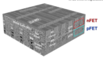
This year there was a late paper from TSMC titled Complementary Field-Effect Transistor (CFET) Demonstration at 48nm Gate Pitch for Future Logic Technology Scaling. A CFET is a CMOS process where the transistors are stacked vertically, rather than being in the same plane as with all previous logic processes: planar, FinFET, nanosheet field effect transistors (NSFET, also known as gate-all-around or GAA). The paper was by about 50 different authors that I’m not going to list, and was presented by Sandy Liao. She said it was “late news” since it is very recent work.
Presumably, TSMC will have a CFET process in the future, but this paper described early research on manufacturability. The process stacks the n-transistor on top of the p-transistor. In the Q&A Sandy was asked what motivated this decision. She said that it wasn’t cast in stone and could get changed in the future, but putting PMOS on the bottom makes handling strain easier. TSMC calls this monolithic CFET or mCFET.
CFET can create an area reduction of 1.5X to 2X, he said. There still has to be space for some vertical routing so you don’t usually get the full 2X you might expect from stacking the transistors. Previous studies of CFET manufacturing have used relaxed gate pitches, and don’t succeed in getting gate pitches around 50nm. So this TSMC study is the first that uses a gate pitch of 48nm, which Sandy said is “pertinent to industry-level advanced node scaling.”
To accomplish this, there is a middle dielectric isolation, inner spacer, and n/p source-drain isolation. This process provides a robust foundation for future mCFET advancement which will require further innovation and additional architectural features.
Here is a TEM demonstration of the mCFET. As I already said, the nFETs are on top and the pFETs on the bottom. Both types of transistors have the channel surrounded by a single metal gate.
Sandy said she would provide some details of the fabrication process “but not too much”. It is a 20-step flow, although obviously there are many sub-steps inside each step. For now, the process is expensive to manufacture she said in time engineers will solve that and so the process will have value. Below are the 20 steps.
By introducing a middle dielectric isolation, inner spacer, and n/p source-drain isolation, the vertically stacked transistors have a survival rate of over 90% with high on-state current and low leakage. There is a six-orders-of magnitude Ion/Ioff current ratio.
Sandy’s conclusion:
This is just the beginning, and there is a long way to go. But transistors in high volume cannot be worse than this. We need work hard to generate process features real yielding circuits with better characteristics.
This is just a study to pave the way for a practical process architecture that can fuel future logic technology, scaling, and PPAC advancement.
I confess I am reading tea leaves in this blog, but why not? Arm recently announced Arm Total Design, an expansion of their Compute Subsystems (CSS) offering which made me wonder about the motivation behind this direction. They have a lot of blue-chip partners lined up for this program yet only a general pointer to multi-die systems and what applications might drive the need. Neither Arm nor their partners will make this investment simply for PR value, so I have to assume there is building activity they are not ready to announce. I’m guessing that in a still shaky economy the big silicon drivers (in hyperscalers, AI, automotive, and maybe communication infrastructure) are already engaged in faster and managed cost paths to differentiated custom silicon, likely in multi-die systems.
Arm CSS and Total Design
I wrote about CSS recently. CSS N2, as Arm describes it, is customizable compute subsystem that is configured, verified, validated and PPA-optimized by Arm. Think of a multi-core cluster objective for which you don’t just get the Lego pieces (CPU core, coherent interconnect, memory subsystem, etc.) but a complete customizable compute subsystem configured with up to 64 Neoverse N2 cores, multiple DDR5/LP DDR5 channels and multiple PCIe/CXL PHY/controller. All verified, validated, and PPA-optimized by Arm to a target foundry and process.
Most recently Arm revealed Arm Total Design, a comprehensive ecosystem of ASIC design houses, IP vendors, EDA tool providers, foundries, and firmware developers – to accelerate and simplify the development of Neoverse CSS-based systems. EDA tools and IP are supplied by Cadence, Synopsys, Rambus and of course Arm, among others. Design services come from companies including ADTechnology, Alphawave Semi, Broadcom, Capgemini, Faraday, Socionext and Sondrel. For silicon process and packaging technology they call out Intel Foundry Services and TSMC (though not Samsung curiously, maybe they are still working on that partnership). And AMI is in this ecosystem to provide software and firmware support.
Reading the tea leaves
I recently blogged on a Synopsys-hosted panel on multi-die systems which suggested already at least 100+ such systems in development. Representatives from Intel and Samsung voiced no objections to that estimate. At the same time there was consensus that these are technologies still very much in development, requiring close collaboration between system company, EDA, IP, chiplet, design services, foundry, and software development. This is not something that an in-house design team, even a hyperscaler design team, can handle on their own.
Arm mentions multi-die chiplet SoC designs in their release though in a fairly general way as the next frontier. I suspect the need is more pressing. Multi-die systems are becoming essential to support state of the art designs driven by the latest AI innovations, especially around transformer-based techniques. We already know that datacenters are pushing these technologies, automotive applications are looking for differentiation in improved natural language recognition and visual transformers for better global recognition, even wireless infrastructure sees application for more intelligent services and more efficient radio communication.
All these applications are pushing higher levels of integration between compute, accelerators and memory, the kind of integration which requires multi-die packaging. This demands experts from foundries to design services to EDA tooling. We also need a ramp-up in available high value chiplet designs, where the press release suggests another hint. Socionext have built a multi-core CPU chiplet around CSS and are aiming it at TSMC 2nm for markets in server CPUs, data center AI edge servers, and 5/6G infrastructure.
More momentum behind multi-die systems. You can read the press release HERE.
The 15th TSMC Open Innovation Platform® (OIP) event was held recently. This event is a focal point across the industry for cutting-edge development and industry-level collaboration. Appropriately, advanced packaging, paving the way for multi-die design was a focal point for the event. You can get a good overview of what was happening at OIP here. Beyond fab and packaging, there was a lot of talk about end markets, with automotive being a key growth area. This is where I’d like to focus in this post – with another example of Analog Bits leadership in automotive grade sensors. Read on to see how Analog Bits leads the way at TSMC OIP with high-accuracy sensors.
Why It’s Important
According to recently published market research, the global automotive sensor market was worth $30.9 B in 2022, and is projected to grow at a CAGR of 7.3% to reach $ 61.4 B from 2023 to 2032. According to the research, “… substantial growth is due to the integration of sensors in vehicles to enhance safety, efficiency, and overall performance. Sensors are used in areas like advanced driver assistance systems (ADAS), engine management, and environmental monitoring. The market’s expansion is driven by regulatory mandates for vehicle safety, the rise of electric and autonomous vehicles, and consumer demand for innovative features.”
The report discussed the need for high-accuracy sensors in automotive designs. Everyone is getting into this market, including:
Robert Bosch GmbH
Continental AG
DENSO Corporation
Analog Devices, Inc.
Sensata Technologies, Inc.
Delphi Automotive PLC
Infineon Technologies AG
STMicroelectronics
The need for high-accuracy, automotive-grade sensors has become a white-hot item in vehicle design. It is against this backdrop that the work presented by Analog Bits is so important.
What Was Presented at OIP
Analog Bits has been at the forefront of precision analog IP for a long time. At OIP, the company showcased numerous IPs on TSMC’s industry-leading N5A process of its new high accuracy sensor and automotive grade, silicon proven designs at its booth. This development is part of Analog Bits’ broadening portfolio of mixed signal IP in advanced TSMC 3nm, 4nm, and 5nm processes. The company announced that design kits are available now.
Mahesh Tirupattur, executive vice president at Analog Bits weighed in with the following official comments:
“As we work with leading edge automotive customers on advanced FinFET processes, thermal issues continue to be a concern and need for multiple instances of sensors continues. Furthermore, many applications cannot have additional test costs associated with trimming for higher accuracy. We have been working on designs for improving un-trimmed accuracy in FinFETs and reducing the area of the sensors, and we are pleased to demonstrate working silicon of these higher accuracy sensors on N5A process at our booth at OIP.”
Mahesh is a force in this industry. You can review his incredible ride at Analog Bits here. Analog Bits has quite a deep technical bench. The president and CTO of Analog Bits, Alan Rogers gave a presentation at OIP about on-die power management IP’s, another very important topic. Let’s look at what Alan presented.
Alan’s Presentation at OIP
Alan Rogers
Alan Rogers has been at Analog Bits for over 25 years, and he’s been working with transistors for over 55 years. In his own words, he’s getting quite good at it. Alan began his presentation with the following introduction:
“In the last 40 years, since my first CMOS chip development in 5u SOS, I’ve watched the power density of silicon chips increase every generation, with higher switching frequencies and larger and larger currents making power integrity a serious design profession. For good reason, the two longest traces on opposite corners of a wire bonded DIP package just don’t seem like a good power delivery solution anymore. How can we help with that? Glad you asked!”
Alan went on to discuss power management challenges in SoCs and chiplets. He covered topics such as the Analog Bits portfolio of on-die power management IP’s, the benefits of this IP, silicon results on TSMC N3E, and future work. He detailed several high-profile challenges being faced by many designers today. These include:
Power integrity and noise
Dynamic power management
Static voltage drop
Heterogeneous integration
Leakage power
Transient voltage spikes and voltage sags
Thermal hazards
He then detailed the various IPs available from Analog Bits to address the above challenges:
PVT Sensors – integrated and pin-less
Power On Reset and Over Current Detection Macro
Power Supply Glitch Detector
Power Supply Droop Detector
Low Dropout Regulator
The impact of a comprehensive library of IP like this can be substantial. Alan touched on some of that impact, including improved power efficiency, faster transient response and efficient regulation, enhanced reliability and improved yield, voltage scalability, integration and space savings, and noise reduction. Quite a list of improvements.
TSMC N3E Test Chip
He then went on to show several actual silicon results from TSMC’s N3E process. The response of the Droop Detector to a slow power slew was shown as well as the linearity of the system against a programmable input threshold. Results over temperature were presented that illustrated the stability and quality of the design. Performance of the PVT sensor was also shown over multiple conditions. The programmability of the Power On Reset macro was shown in detail as well.
Overall, an impressive portfolio of IP and an impressive set of results on an advanced process.
To Learn More
If you’d like to dig into the array of precision IPs offered by Analog Bits, you can do so here. And that’s how Analog Bits leads the way at TSMC OIP with high-accuracy sensors.
TSMC has been offering foundry services since 1987, and their first 3nm node was called N3 and debuted in 2022; now they have an enhanced 3nm node dubbed N3E that has launched. Every new node then requires IP that is carefully designed, characterized and validated in silicon to ensure that the IP specifications are being met and can be safely used in SoC or multi-die system designs. This new IP must cover a wide range of functions, like interface, memory and logic. Synopsys has a large IP team that has risen to the challenge by creating new IP for the TSMC N3E node and achieving first-pass silicon success.
Chiplet Interconnect
Systems made up of heterogeneous chiplets require die-to-die communication, and that’s where the UCIe standard comes into play. Synopsys is a Contributor member of the UCIe Consortium, and they offer IP for both a UCIe Controller and a UCIe PHY in the TSMC N3E node.
The UCIe PHY IP had first silicon results in August 2023, showing data rates of 16Gbps and scalable to 24Gbps per channel. . Earlier this year, Intel unveiled world’s first Intel-Synopsys UCIe interoperability test chip demo at Intel Innovation. The interoperability was between Synopsys UCIe PHY IP on TSMC N3E process and Intel PHY IP on Intel 3 technology.
Industry’s Broadest Interface IP Portfolio on TSMC N3E
The IEEE approved the 802.3 standard for Ethernet back in 1983, quite the extended standard, while the Synopsys 224G Ethernet PHY IP had first silicon success in August 2023. Network engineers look at the eye diagram to see the 224Gbps PAM-4 encoding. Jitter levels surpassed both the IEEE 802.3 and OIF standard specifications.
Supporting standards like PCI Express 6.0, 400G/800G Ethernet, CCIX, CXL 2.0/3.0, JESD204 and CPRI there is the Synopsys Multi-Protocol 112G PHY IP. Engineers can combine this PHY IP with a MAC and PCS to build a 200G/400G/800G Ethernet block.
SDRAM and memory modules can use the Synopsys DDR5 PHY IP on TSMC N3E to achieve transfer rates up to 8400Mbps. You can see the wide open eye and clear margins for this IP operating at speed.
The PCI Express standard started out in 2003 and has been continually updated to meet the growing demands of cloud computing, storage, and AI. PCIe 5.0 is now supported using the Synopsys PCIe 5.0 PHY IP. First silicon on TSMC N3E showed operating speeds of 32 GT/s, and the Synopsys PCIe 5.0 PHY IP is listed on the PCI-SIG Integrators list.
I’ve been using USB-C on my MacBook Pro, iPad Pro and Android phone for years now. Synopsys now supports USB-C 3.2 and DisplayPort 1.4 PHY IP in the latest TSMC process. With this IP users can connect up to 8K Ultra High-Definition displays.
Smartphone companies standardized on the MIPI protocol years ago as an efficient way to connect cameras, and the Synopsys MIPI C-PHY IP/D-PHY IP can operate at 6.5Gb/s per lane and 6.5Gs/s per trio. The C-PHY IP supports v2.0, and the D-PHY IP2.1.
The latest Synchronous DRAM controller spec is LPDDR5X, supporting data transfer speeds up to 8533Mbps, a 33% improvement over LPDDR5 memory. The Synopsys LPDDR5X/5/4X Controller is silicon-proven, and ready to be designed with.
Logic Libraries and Memories
Up to half the area of an SoC can be memories, so the good news is that the Synopsys Foundation IP allows you to add memories and logic library cells quickly into a new design. Here are the test chip diagrams from Synopsys on the TSMC N3E node for memories and logic libraries.
Summary
TSMC and Synopsys have collaborated quite well together over the years, and that partnership now extends to the N3E node where SoC designers can find silicon-tested IP for interfaces, memories and logic. Power, performance and yield are looking attractive for N3E, so the technology is ready for your most demanding designs. Starting a design with N3E also provides you a quicker path to migrate to the N3P process.
Instead of creating all of your own IP from scratch, which will lengthen your schedule, require more engineering resources and increase risk, why not take a look at the proven and broad Synopsys IP portfolio for N3E .
The 15th TSMC Open Innovation Platform® (OIP) was held last week. In preparation we did a podcast with one of the original members of the TSMC OIP team Dan Kochpatcharin. Dan and I talked about the early days before OIP when we did reference flows together. Around 20 years ago I did a career pivot and focused on Strategic Foundry Relationships. The importance of the foundries was clear to me and I wanted to be an integral part of that ecosystem. As it turns out it was a great career move, absolutely.
Before I get to the importance of the early TSMC reference flow days let’s talk about the recent OIP event. It was held at the Santa Clara Convention Center and it was a full house. For those other semiconductor event coordinators, if you want full semiconductor attendance use the Santa Clara Convention Center. Local hotels or the San Jose Convention Center are not convenient and convenience means attendance. TSMC switched to the Santa Clara Convention Center from San Jose a few years back and the rest as they say is history, TSMC hosts the best semiconductor networking events.
This year OIP was all about packaging and rightly so. It is the next foundry battleground and TSMC is once again building a massive ecosystem appropriately named the 3D Fabric Alliance:
“As the industry shifted toward embracing 3D IC and system-level innovation, the need for industry-wide collaboration has become even more essential than it was when we launched OIP 15 years ago,” said Dr. L.C. Lu, TSMC fellow and vice president of Design and Technology Platform. “As our sustained collaboration with OIP ecosystem partners continues to flourish, we’re enabling customers to harness TSMC’s leading process and 3DFabric technologies to reach an entirely new level of performance and power efficiency for the next-generation artificial intelligence (AI), high-performance computing (HPC), and mobile applications.”
L.C. Lu has been part of the TSMC OIP since the beginning, he worked for Dr. Cliff Hou. From 1997 to 2007 Cliff established the TSMC PDK and reference flow development organizations which then led to the OIP. Cliff Hou is now TSMC Senior Vice President, Europe & Asia Sales and Research & Development / Corporate Research.
L.C. updated us on the progress of the 3D Alliance and 3D Blox which is an incredible piece of technology that is open to all customers, partners and competitors alike. It is an industry standard in the making for sure. We covered 3D Blox HERE and TSMC gave us this update:
Introduced last year, the 3Dblox open standard aims to modularize and streamline 3D IC design solutions for the semiconductor industry. With contribution from the largest ecosystem of companies, 3Dblox has emerged as a critical design enabler of future 3D IC advancement.
The new 3Dblox 2.0, launched today, enables 3D architecture exploration with an innovative early design solution for power and thermal feasibility studies. The designer can now, for the first time in the industry, put together power domain specifications and 3D physical constructs in a holistic environment and simulate power and thermal for the whole 3D system. 3Dblox 2.0 also supports chiplet design reuse features such as chiplet mirroring to further improve design productivity.
3Dblox 2.0 has won support from key EDA partners to develop design solutions that fully support all TSMC 3DFabric offerings. Those comprehensive design solutions provide designers with key insights to make early design decisions, accelerating design turnaround time from architecture to final implementation.
TSMC also launched the 3Dblox Committee, organized as an independent standard group, with the goal to create an industry-wide specification that enables system design with chiplets from any vendors.Working with key members including Ansys, Cadence, Siemens, and Synopsys, the committee has ten technical groups of different subjects and proposes enhancements to the specs and maintain the interoperability of EDA tools. Designers can now download the latest 3Dblox specifications from the 3dblox.org website and find more information about 3Dblox and its tool implementation by EDA partners.
Back to the reference flows, I was the Strategic Foundry Relationship Advisor for Solido Design Automation out of Saskatoon Canada and Berkeley Design Automation (BDA) in Silicon Valley at the time. Back then EDA included a lot of point tools inside the design flow since no one company could do it all. So all of the point tool companies looked to TSMC for guidance on how to interoperate inside a customer’s design flow. This was not only valuable experience, it provided much needed exposure for EDA start-ups to the TSMC customer base. In the case of Solido and BDA, it not only led to rapid adoption by TSMC’s top customers, TSMC itself licensed the tools for internal use which is the ultimate seal of approval. Solido and BDA were both acquired by Seimens EDA and their close relationships with TSMC was a big part of that transaction, believe it.
A similar process was developed for silicon proven IP. I am also a Foundry Relationships Advisor for IP companies and not only do we get access to TSMC’s top customers, TSMC allows access to PDKs and taught us how to silicon prove our products. Notice on the TSMC OIP partner list the biggest market segment is IP companies for these exact reasons. IP is a critical enabler for the foundry business and getting silicon right the first time is what OIP is all about.
Bottom line: In the foundry business it’s all about collaboration and TSMC built this massive ecosystem from the ground up. Not only does it reduce customer risk of designing to new processes, the close collaboration between TSMC and the ecosystem partners multiplies the total annual ecosystem R&D investments exponentially.
TSMC originally brought the pure-play foundry business to the United States in 1996 through a joint venture with customers Altera, Analog Devices, ISSI, and private investors (no government money). Altera is now part of Intel but ADI is still a top TSMC customer and enthusiastic supporter. I have seen the ADI CEO Vincent Roche present at recent TSMC events and his TSMC partnership story is compelling. This joint venture was part of TSMC’s customer centric approach to business, responding directly to customer requests.
The WaferTech fab was established in Camas Washington (just North of the Oregon/Washington border) in 1996 with an investment of more than $1B which was a huge amount of money at the time. Production started two years later at .35 micron which was part of the Philips technology transfer that TSMC was founded upon. In 2000 TSMC bought out the partners and private investors, taking full control of the Washington fab. It is now called TSMC Fab 11 but clearly this fab was ahead of its time, absolutely.
WaferTech focuses on Embedded Flash process technology while supporting a broad TSMC technology portfolio on line-widths ranging from 0.35-microns down to 0.16-microns. We specialize in helping companies deliver differentiated products and work with them on a number of customized and manufacturing “phase-in” projects. As a result, WaferTech delivers the latest generation semiconductors around the globe, supporting innovations in automotive, communications, computing, consumer, industrial, medical and military/aerospace applications.
To complement our world class process manufacturing services, WaferTech also provides test and analysis services at our Camas, Washington facility. Moreover, TSMC provides design, mask and a broad array of packaging and backend services at its other locations around the world. WaferTech also is a host for TSMC’s foundry-leading CyberShuttle™ prototyping services that help reduce overall design risks and production costs.
“With WaferTech on-line and shipping, TSMC customers gain another assured source for wafers produced to our standards of excellence,” said Ron Norris, president of TSMC, USA and a director of WaferTech. “Now TSMC is the only foundry in the world to transparently support customers from geographically dispersed sites.”
Ron Norris is another hire TSMC made with TI roots. Ron himself was a semiconductor legend. He started his career at TI and held executive level positions at Microchip in Arizona, Fairchild Semiconductor in Silicon Valley, and Data I/O Systems in Redmond WA, so he certainly knew the challenges of semiconductor manufacturing in the United States.
Historically, TSMC doesn’t just build fabs, TSMC builds communities. In fact, a TSMC fab itself is a community with everything you need to help maintain a work life balance. I have spent a lot of time in different fabs around the world but for the most part they were TSMC fabs in Taiwan. I still consider the Hsinchu Hotel Royal (walking distance from TSMC Fab 12A) as my second home. I remember flying in on my birthday one year and the staff had a mini birthday celebration when I arrived. Yes, they are that good, but I digress.
One thing you have to remember is that in Taiwan, working for TSMC brings status. You are a rockstar. Working for Samsung in South Korea has a similar aura. When TSMC breaks ground on a new fab location in Taiwan you can expect a whole support ecosystem to develop around it with everything a TSMC fab needs to be successful including housing and university level education for recruiting and employee growth.
Bottom line: Working for TSMC in Taiwan is like joining a very large and very successful family business.
Unfortunately, in Camas Washington, that was not the case. The WaferTech campus is a 23 acre complex housed on 260 acres. The main fabrication facility consists of a 130,000 square foot 200mm wafer fabrication plant. Additional fabs were planned but never built, a support ecosystem never formed, thus the TSMC Taiwan fab recipe was called out as a failure in the US.
Many reasons have been sited for this “failure” including high costs, problems attracting local talent, and timing (soft economy), but in my opinion it also had a lot to do with the rockstar factor. In the US we had forgotten or did not know yet how important semiconductors were to modern life and TSMC was not a big name in the US like it is today.
Now that TSMC is building fabs in Arizona, Kumamoto Japan, and Dresden Germany it will be interesting to see how different the TSMC experience is in these world wide locations.