At the TSMC Technology Symposium last month Suk Lee presented a lot of information on design enablement. Suk is an interesting guy with a unique background in ASIC, Semiconductor, EDA, and now Foundry. In baseball terms that would be like playing infield, outfield, home plate, and umpire!
Around the turn of the millennium Suk actually worked for me. In fact, he took over my job running marketing for IC, which is what Cadence called all of the back end tools for both analog and digital. After that he went to Magma (which of course was acquired by Synopsys). At the start of his career he had also, like me, worked for an ASIC semiconductor company, VLSI Technology in my case and LSI Logic for Suk, so we both have what I like to call “silicon in our veins”. That was followed by his first stint at Cadence before going back to semiconductor at Texas Instruments. He joined TSMC six years ago where he is now senior director of design infrastructure marketing, based in Taiwan.
First there are the new 28nm processes, 28HPC+ and 28ULP. 28HPC+ is for high performance, a speed gain of about 15% for the same leakage, or a reduction of 30-50% in leakage for the same speed. There are also new standard cell libraries for this process with 9 and 7 track libraries (compared to 12T/9T before). The 28ULP (for ultra-low power) process is for IoT applications with a lower operating voltage of 0.7V (versus 0.9V for 28HPC+). This new process joins the other two ULP processes 55ULP and 40ULP. There is also a library benchmarking kit to help design groups find the best combination of libraries to meet their target PPA.
The design flows are largely in place for both processes. The foundation IP is ready for 28HPC+ with other IP becoming available from now through Q1 of next year. A lot of the IP for 28ULP is still in the planning phase.
Next Suk talked about the 16FF+. The design flows and IP portfolio are all in place with almost everything characterized in silicon. At the event a new 16nm process 16FFC was announced. This is intended for cost-sensitive consumer applications. The foundation IP should be available in Q4 of this year, with interface IP coming in Q2 of 2016.
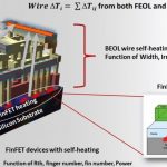
There was a lot of detailed information about 10nm which TSMC were talking about for the first time.
EDA tool support is as follows:
- Automatic Place & Route: Synopsys, Cadence, Mentor
- DRC: Synopsys, Cadence, Mentor
- LVS: Synopsys, Cadence, Mentor
- RCX: Synopsys, Cadence, Mentor
- STA: Synopsys, Cadence
- EM/IR: Synopsys, Cadence, Ansys
- SPICE: Synopsys, Cadence, Mentor
- FastSpice: Synopsys, Cadence, Mentor
- Custom Design: Synopsys, Cadence
The IP library for 10FF is targeted at several different application areas: smartphone, tablet/ultrabook, networking, CPU/GPU/FPGA. The various IP very in their state of readiness from being full characterized from silicon test chips, or waiting for silicon characterization (but able to be used in design starts), to blocks that are still in development. In detail, IP for 10FF is available as follows:
- Standard cell: silicon report
- GPIO/ESD: silicon report
- PLL: pre-silicon design kit
- SRAM compiler: silicon report
- ROM compiler: in development
- Electrical fuse: silicon report
- OTP: in development
- DDR4: pre-silicon design kit
- LPDDR4: pre-silicon design kit
- PCIe: pre-silicon design kit G3 & G4
- MIPI: pre-silicon design kit G2 & G3
- SATA II/III: in development
- 10G serdes: in development
- USB 2/3: pre-silicon design kit
- HDMI/MHL/DP: in development
The 3DIC technologies offer offer heterogeneous die stacking and packaging solutions for high speed, high density and low cost applications. There is thru-silicon-via (TSV) implementation with accurate modeling, an integrated 3D testing methodology, wide-IO interface signal integrity and chip-package-system thermal analysis. The design flow is completely ready, with design kits ready.
TSMC has the broadest IP portfolio in the industry with IP from 0.35um down to 10nm with nearly 9000 different IP titles.
The China Symposium is next week in Shanghai on 5/7 (in Chinese). European symposia are in Amsterdam on 6/16 and Herzliya on 6/29. The TSMC symposium page is here. There will be one in Yokohama but the date is not yet decided. But save the date 9/19 for the OIP Ecosystem Forum in Santa Clara. Details are here.