As I mentioned in my previous post, the TSMC investor call this month was very interesting and Morris Chang was in fine form during the Q&A. As a semiconductor professional I think some of the questions are ridiculous but maybe they have value to the financial people. This one question from Randy, who I think is very astute, is SemiWiki discussion worthy:
Randy Abrams
Yes, thank you. The first question, I wanted to ask your outlook is more in line with the industry where you are guiding 5% to 10% for foundry near similar levels. Could you talk about the factors to be more inline after gaining the last few years? And can you also address the China business; we are seeing the China foundries grow faster. SMIC is growing 20% to 30%, how does TSMC combat or defend share more on the mature nodes, where they’re starting to grow faster?
(At the bottom it says SMIC is partially owned by TSMC. TSMC did get a 10% equity stake after the IP litigation which I thought TSMC had already divested. Please post a comment if you know otherwise.)
First and foremost, TSMC is being conservative as they always are and they are shielding their #1 customer which is Apple. There is no way the second half of the year will be 5% growth with Apple single sourcing 10nm from TSMC for the next iPhone and iPad. TSMC will again be in double digits (10-15% revenue growth) for 2017 as I previously stated.
This is going to be another strong year for the foundries but I do find it interesting that while the semiconductor foundry business is posting double digit gains the semiconductor industry as a whole is relatively flat… Comments?
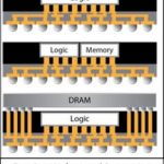
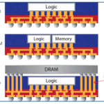
Second, SMIC is surging on 2[SUP]nd[/SUP] source business now that they are shipping a TSMC compatible 28nm, most of which is in China. How does TSMC combat or defend the mature nodes? In China they don’t, they push the market to FinFETs. Remember, the TSMC GDS compatible market stops with FinFETs and SMIC does not expect to have 14nm until 2020 or so. Meanwhile TSMC is getting ready to release a fourth generation (12nm) FinFET process optimized for density and cost. In fact, I hope TSMC shows an updated version of the infamous Intel chip scaling graph shown below.
Remember, this graph was based on a paper done by TSMC before 16nm went into production. TSMC then released 16FF+, 16FFC, and now 12nm.
My guess is that TSMC 12nm will easily be on par with Intel 14nm in regards to chip density and superior in cost per transistor… Comments?
Unfortunately, Intel is still flogging this outdated slide. In fact, just this month at the J.P. Morgan 2017 Tech Forum, Intel Client Computing Group VP Navin Shenoy said Intel 14nm is equivalent to Samsung and TSMC 10nm so they are considering renaming their 10nm:
“I’m confident that when 10 nanometer — our 10 nanometer — comes out, and this is something that maybe we should rename it, I don’t know, we’ll think about that, but when our 10 nanometer comes out, we will have a clear density advantage, and a clear performance and power advantage versus what others in the industry have.”
Well, yes and no. Unfortunately for Intel their 10nm will come out about the same time as TSMC 7nm so no, Intel will not have a clear density advantage:
Morris Chang
I think 2017 will be pretty strong in terms of technology, it will be a pretty strong 16 or 14 FinFET year, and our market share in 16, while it’s quite high, is not as high as I would like, it’s actually in the close to 70% or 65% to 70%. Now that is not quite as high as our 28 nanometer which even now, you know, like almost 80% and now, 2017 is – I think it’s a pretty – we think will be a pretty strong year and result.
Absolutely…