TSMC 5nm and EUV Update 2018

TSMC 5nm and EUV Update 2018
by Daniel Nenni on 01-23-2018 at 12:00 pm

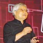
The TSMC Q4 2017 earnings call transcript is up and I found it to be quite interesting for several reasons. First and foremost, this is the last call Chairman Dr. Morris Chang will participate in which signifies the end of a world changing era for me and the fabless semiconductor ecosystem, absolutely. TSMC announced his retirement with Mark Liu, who has been co-CEO along with C.C. Wei since 2013, replacing Morris as Chairman and C.C. Wei taking over the role of single CEO. Earnings calls were much more interesting when Morris Chang participated especially in the Q&A session when he questioned some of the questions. Here is his good-bye:

I really have spent many years with some of you, many years, more than 20 years. Although I think most of you probably haven’t attended this particular conference that long. But having here almost 30 years I think, yes. And I enjoyed it, and I think that we all — at least I hope that I had a good time. I hope that you had a good time, too. And I will miss you, and thank you very, very much. Thank you. Thank you. Thank you.

The call started out with Laura Ho and financial recaps but also revenue by technology:

10-nanometer process technology continues to ramp strongly, accounted for 25% of total wafer revenue in the fourth quarter. The combined 16/20 contribution was 20% of total wafer revenue. Advanced technologies, meaning 28-nanometer and below, accounted for 63% of total wafer revenue, up from 57% in the third quarter. On a full year basis, 10-nanometer contribution reached 10% of total wafer revenue in 2017. The combined 16 and 20 contribution was 25% of total wafer revenue. Advanced technology, 28-nanometer and below, accounted for 58% of total wafer revenue, up from 54% in 2016.

This really is good news for TSMC since the more mature nodes (40nm and above) are more competitive thus lower margined. It will be interesting to see when TSMC lowers that advanced node bar below 28/22nm, probably in two years when 7nm hits HVM and 5nm is ramping.

Laura ended her remarks with a solid Q1 guidance:

Based on the current business outlook, we expect first quarter revenue to be between USD 8.4 billion and USD 8.5 billion, which is an 8.3% sequential decline but a 12.6% year-over-year increase at the midpoint and represent a new record high in terms of first quarter revenue.

Mark Lui started his prepared remarks with an introduction to the TSMC “Everyone’s Foundry” strategy:

Firstly, I would like to talk about our “Everyone’s Foundry” strategy. Being everyone’s foundry is the strategy TSMC takes by heart. Through our technology and services, we build an Open Innovation Platform, where all innovators in the semiconductor industry can come to realize their innovation and bring their products to life. As our customers continue to innovate, they bring new requirements to us, and we need to continuously develop new capabilities to answer them. In the meantime, they utilize those shared capabilities such as yield improvement, design, utilities, foundation IPs and our large-scale and flexible capacities. In this way, this open innovation ecosystem expands its scale and its value. We do not compete with our customers. We are everyone’s foundry.

The translation here in Silicon Valley is that TSMC does not compete with customers or partners which is a direct shot at Samsung, my opinion. Mark also talked about the latest semiconductor killer app and that is cryptocurrency mining which is booming in China:

Now on cryptocurrency demand: In the past, TSMC’s open innovation ecosystem incubates numerous growth drivers for the semiconductor industry. In the ’90s, it was the PC chipsets; then in the early ’20s, the graphic processors; in the mid- to late ’20s, it was chipset for cellular phone; recently, start 2010, it was for smartphones. Those ways of innovation continuously sprout in our ecosystem and drive the growth of TSMC. Furthermore, we are quite certain that deep learning and blockchain technologies, which are the core technology of cryptocurrency mining, will lead to new waves of semiconductor innovation and demand for years to come.

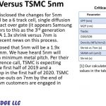
Mark then switched to 5nm (N5) and EUV readiness. According to Mark, N5 is on track for Q1 2019 risk production which gives plenty of room for Apple to get 5nm SoCs out in time for 2020 Apple products. I have not heard any fake news about Apple switching foundries which is a nice change. TSMC and Apple are like peanut butter and jelly…

EUV is also progressing with high yields on N7+ and N5 development. Some customers have mentioned getting EUV at the contacts and vias at 7N before getting EUV for metals and shrink at 7N+ which makes complete sense to me.

Mark also mentions that EUV source power is at 160 watts for N7 with N5 development activities at 250 watt waiting in the wings. This all jives with what Scott Jones presented at ISS 2018 last week. Mark’s EUV pellicle comment however left me with a question:

EUV pellicle making has also been established with low defect level and good transmission properties. So we are confident that our EUV technology will be ready for high-volume production for N7+ in 2019 and N5 in 2020.

I’m curious to know what “good transmission properties” are. From what I am told they need to be 90%+ but they are currently in the low 80% range. Does else anybody know? Can someone share their pellicle wisdom here? The other EUV question I have is about the 10% performance and density gain between 7N and 7N+. Is that EUV related or just additional process optimization? I will be in Hsinchu next week so I can follow-up after that.

All-in-all it really was a good call, you can read the full transcript HERE.


ISS 2018 – The Impact of EUV on the Semiconductor Supply Chain

ISS 2018 – The Impact of EUV on the Semiconductor Supply Chain
by Scotten Jones on 01-18-2018 at 8:00 am

I was invited to give a talk at the ISS conference on the Impact of EUV on the Semiconductor Supply Chain. The ISS conference is an annual gathering of semiconductor executives to review technology and global trends. In this article I will walk through my presentation and conclusions.
Continue reading “ISS 2018 – The Impact of EUV on the Semiconductor Supply Chain”


ASIC and TSMC are the AI Chip Unsung Heroes

ASIC and TSMC are the AI Chip Unsung Heroes
by Daniel Nenni on 11-20-2017 at 7:00 am

One of the more exciting design start market segments that we track is Artificial Intelligence related ASICs. With NVIDIA making billions upon billions of dollars repurposing GPUs as AI engines in the cloud, the Application Specific Integrated Circuit business was sure to follow. Google now has its Tensor Processing Unit, Intel has its Nervana chip (they acquired Nervana), and a new start-up Groq (former Google TPU people) will have a chip out early next year. The billion dollar question is: Who is really behind the implementations of these AI chips? If you look at the LinkedIn profiles you will know for sure who it isn’t.

The answer of course is the ASIC business model and TSMC.

Case in point: eSilicon Tapes Out Deep Learning ASIC

The press release is really about FinFETs, custom IP, and advanced 2.5D packaging but the big mystery here is: Who is the chip for? Notice the quotes are all about packaging and IP because TSMC and eSilicon cannot reveal customers:

“This design pushed the technology envelope and contains many firsts for eSilicon,” said Ajay Lalwani, vice president, global manufacturing operations at eSilicon. “It is one of the industry’s largest chips and 2.5D packages, and eSilicon’s first production device utilizing TSMC’s 2.5D CoWoS packaging technology.”

“TSMC’s CoWoS packaging technology is targeted for the kind of demanding deep learning applications addressed by this design,” said Dr. BJ Woo, TSMC Vice President of Business Development. “This advanced packaging solution enables the high-performance and integration needed to achieve eSilicon’s design goals.”

From what I understand, all of the chips mentioned above were taped-out by ASIC companies and manufactured at TSMC. It will be interesting to see what happens to the Nervana silicon now that they are owned by Intel. As we all now know, moving silicon from TSMC to Intel is much easier said than done.

The CEO of Nervana is Naveen Rao, a very high visibility semiconductor executive. Naveen started his career as a design and verification engineer before switching to a PhD in Neuroscience and co-founding Nervana in 2014. Intel purchased Nervana two years later for $400M and Naveen now leads AI products at Intel and has published some very interesting blogs on being acquired and what the future holds for Nervana.

You should also check out the LA Times article on Naveen:

Intel wiped out in mobile. Can this guy help it catch the AI wave?

Rao sees a way to surpass Nvidia with chips designed not for computer games, but specifically for neural networks. He’ll have to integrate them into the rest of Intel’s business. Artificial intelligence chips won’t work on their own. For a time, they’ll be tied into Intel’s CPUs at cloud data centers around the world, where Intel CPUs still dominate — often in concert with Nvidia chips…

Groq is even more interesting since 8 of the first 10 members of the Google TPU team are founders, which is the ultimate chip “do over” scenario, unless of course Google lawyers come after you. If you don’t know what Groq means check the Urban Dictionary. I already know because I was referred to as Groq after starting SemiWiki, but not in a good way.

If you check the Groq website you will get this stealthy screenshot:

But if you Google Groq + Semiconductor you will get quite a bit of information so stealthy they are not. The big ASIC tip-off here is that while at Google they taped out their first TPU in just over a year and the Groq chip will be out in less than two years with only $10M in funding.

So please, let’s all give a round of applause to the ASIC business model and give credit where credit is due, absolutely.


Also Read:

AI ASICs Exposed!

Deep Learning and Cloud Computing Make 7nm Real


TSMC EDA 2.0 With Machine Learning: Are We There Yet ?

TSMC EDA 2.0 With Machine Learning: Are We There Yet ?
by Alex Tan on 11-06-2017 at 7:00 am

Recently we have been swamped by news of Artificial Intelligence applications in hardware and software by the increased adoption of Machine Learning (ML) and the shift of electronic industry towards IoT and automobiles. While plenty of discussions have covered the progress of embedded intelligence in product roll-outs, an increased focus on applying more intelligence into the EDA world is required.

Earlier this year TSMC reported successful initial deployment of machine learning on ARM A72/73 cores in which it helps predict an optimal cell clock-gating to gain overall chip speeds of 50 – 150 MHz. The techniques include training models using open source algorithms maintained by TSMC.


In ISPD 2017
,TSMC referred to this platform as the ML Design Enablement Platform. ​It was anticipated to allow designers to create custom scripts to cover other designs.

During the
2017 CASPA Annual Conference, Cadence Distinguished Engineer, David White shared his thoughts on the current challenges faced by the EDA world which consists of 3 factors:

  • Scale – with increasing design sizes, more rules/restrictions and massive data such as simulation, extraction, polygons, technology files are expected.
  • Complexitymore complex FinFET process technologies resulting in complicated DRC/ERC, while pervasive interactions between chip and packaging/ board becoming the norm. On the other hand thermal physical effect between devices and wires is needing attention.
  • Productivityintroduce uncertainty and more iterations while limited retrained design and physical engineers.

Furthermore, David categorized the pace of ML (or Deep Learning) adoption into 4 phases:


Although the EDA industry has started embracing ML as a new venue to enhance their solutions this year, the question is: How far have we gone? During 2017 Austin DAC, several companies announced augmenting ML in their product offerings as shown in table 2.


You might have heard the famous quote, “War is 90% information“. ML adoption may require good data analytics as one is faced with paramount data size to handle. For most hardware products augmenting ML can be either done on the edge (gateway) or in clouds. With respect to the EDA tools, it also becomes a question of how massive and accurate the trained models need to be and whether it requires many iterations.

For example, predicting the inclusion of via pillar in a FinFET process node could be done at a different stage of design implementation while the model accuracy should be validated at post-route. Injecting them during placement would be different than in physical synthesis where there is still no concept of legalized design and projected track usage.

Let’s revisit David’s presentation and find out what steps are required to design and develop intelligent solutions which involve harnessing ML, analytics and clouds, coupled with prevailing optimizations. He believes it’s comprised of two phases: training development phaseand operational phase.Each implies certain context as shown in the following snapshot (training = data preparation + model based inference; operational = adaptation).


The takeaways from David’s formulation involve properly managing data preparation to reduce its size prior to generating, training, and validating the model. Once completed, the calibration and integration to the underlying optimization or process can take place. He believes that we are just starting phase 2 in augmenting ML into EDA (refer to table 1).

Considering the increased attention given to ML during 2017 TSMC Open Innovation Platform, in which TSMC explored the use of ML to apply path-grouping during P&R to improve timing and Synopsys MLadoption to predict potential DRC hotspots, we are on the right track to have smarter solutions to balance the complexity challenges to high density and finer process technology.


Deep Learning and Cloud Computing Make 7nm Real

Deep Learning and Cloud Computing Make 7nm Real
by Daniel Nenni on 11-05-2017 at 7:00 am

The challenges of 7nm are well documented. Lithography artifacts create exploding design rule complexity, mask costs and cycle time. Noise and crosstalk get harder to deal with, as does timing closure. The types of applications that demand 7nm performance will often introduce HBM memory stacks and 2.5D packaging, and that creates an additional long list of challenges. So, who is using this difficult, expensive technology and why?

A lot of the action is centering around cloud data center buildout and artificial intelligence (AI) applications – especially the deep learning aspect of AI. TSMC is teaming with ARM and Cadence to build advanced data center chips. Overall, TSMC has an aggressive stance regarding 7nm deployment. GLOBALFOUNDRIES has announced 7nm to support for, among other things, data center and machine learning applications, details here. AMD launched a 7nm GPU with dedicated AI circuitry. Intel plans to make 7nm chips this year as well. If you’re wondering what Intel’s take is on AI and deep learning, you can find out here. I could keep going, but you get the picture.

It appears that a new, highly connected and automated world is being enabled, in part, by 7nm technology. There are two drivers at play that are quite literally changing our world. Many will cite substantial cloud computing build-out as one driver. Thanks to the massive, global footprint of companies like Amazon, Microsoft and Google, we are starting to see compute capability looking like a power utility. If you need more, you just pay more per month and it’s instantly available.

The build-out is NOT the driver however. It is rather the result of the REAL driver – massive data availability. Thanks to a new highly connected, always-on environment we are generating data at an unprecedented rate. Two years ago, Forbes proclaimed: “more data has been created in the past two years than in the entire previous history of the human race”. There are other mind-blowing facts to ponder. You can check them out here. So, it’s the demand to process all this data that triggers cloud build-out; that’s the core driver.

The second driver is really the result of the first – how to make sense out of all this data. Neural nets, the foundation for deep learning, has been around since the 1950s. We finally have data to analyze, but there’s a catch. Running these algorithms on traditional computers isn’t practical; it’s WAY too slow. These applications have a huge appetite for extreme throughput and fast memory. Enter 7nm with its power/performance advantages and HBM stacks. Problem solved.

There is a lot of work going on in this area, and it’s not just at the foundries. There’s an ASIC side of this movement as well. Companies like eSilicon have been working on 2.5D since 2011, so they know quite a bit about how to integrate HBM memory stacks. They’re also doing a lot of FinFET design these days, with a focus down to 7nm. They’ve recently announced quite a list of IP targeted at TSMC’s 7nm process. Here it is:

Check out the whole 7nm IP story. If you’re thinking of jumping into the cloud or AI market with custom silicon, I would give eSilicon a call, absolutely.


Choosing the lesser of 2 evils EUV vs Multi Patterning!

Choosing the lesser of 2 evils EUV vs Multi Patterning!
by Robert Maire on 11-03-2017 at 12:00 pm

For Halloween this week we thought it would be appropriate to talk about things that strike fear into the hearts of semiconductor makers and process engineers toiling away in fabs. Do I want to do multi-patterning with the huge increase in complexity, number of steps, masks and tools or do I want to do EUV with unproven tools, unproven process & materials and little process control?
Continue reading “Choosing the lesser of 2 evils EUV vs Multi Patterning!”


Arm TechCon Preview with the Foundries!

Arm TechCon Preview with the Foundries!
by Daniel Nenni on 10-23-2017 at 9:00 am

This week Dr. Eric Esteve, Dr. Bernard Murphy, and I will be blogging live from Arm TechCon. It really looks like it will be a great conference so you should see some interesting blogs in the coming days. One of the topics I am interested in this year is foundation IP and I will tell you why.

During the fabless transformation of the semiconductor industry, semiconductor IP became a key enabler with EDA tools and ASIC services. Today, as non-traditional chip companies start designing chips from scratch, Foundation IP (SRAM, Standard Cells, and I/Os) from leading IP companies will again be front and center and when you want to know the latest about Foundation IP you talk to the foundries, absolutely.

In case you did not know, one of our leading foundry executives recently moved to Semiconductor IP which will bring a whole new perspective. Kelvin Low started at Chartered Semiconductor, then GLOBALFOUNDRIES, followed by Samsung Foundry, and is now Vice President of Marketing at Arm Physical Design Group where he will soon celebrate his 20th year in semiconductors. I had lunch with Kelvin recently and he told me what to look for in regards to foundries this week at Arm TechCon which starts with a free lunch with TSMC, Cadence, Xilinx, and Arm:

Unprecedented Industry Collaboration Delivers Leading 7nm FinFET HPC Solutions
Join us for an ecosystem lunch and joint presentations from our Ecosystem partners focusing on FinFET collaboration!In the first section of this set of four sessions, you will hear how Arm® and its Ecosystem partners delivered industry-leading 7nm FinFET solutions to address applications of the High Performance Computing (HPC) segment. With the implementation complexity at small geometries and more demanding product requirements, it is imperative that the Ecosystem collaborate closely to meet the most stringent system-level performance and power targets. Speakers from TSMC®, Cadence®, Xilinx® and Arm will share details of our combined effort and discuss key challenges and future opportunities.

Transforming Markets with Arm and Intel FinFET Solutions
In the second of four sessions, extend your lunch with us to hear from Arm and Intel® on our new partnership focusing on our collaborative solutions for 10hpm and 22ffl. The second part of the sponsored session covers the joint strategy bringing Arm and Intel Custom Foundry to the ecosystem. Together, we will share our planned journey to enable smart mobile computing on these key process nodes. Speakers from Arm and Intel will also discuss co-optimization of the process technology, and how we will expand the collaboration for broader solutions.

Samsung Foundry Roadmap to Advanced FinFET Nodes
In the third of four sessions, we welcome presenters from Samsung Foundry and Arm. Samsung Foundry will showcase their latest FinFET roadmap at 14nm, 11nm and beyond, including the value proposition and target markets for their advanced nodes. Samsung and Arm will highlight the results of our collaborative efforts in this space with Arm detailing their 14LPP and 11LPP platform offering and support of the Samsung Foundry roadmap for the benefit of the ecosystem.

Arm Physical Design Solutions
In the fourth of four sessions, we invite you to close out your lunch and hear direct from Arm on our physical design solutions for the ecosystem. We will cover cross-foundry roadmaps with a focus on POPTM IP, bring new optimizations to Arm CortexTM-A cores targeting improved design turnaround time. And we have an exciting announcement for our product availability on DesignStart.

If you would like to meet us at Arm TechCon message us on SemiWiki and I will make sure it happens. You can meet me in the Open-Silicon booth #918 Wednesday morning where we will be giving away 300 copies of Custom SoCs for IoT: Simplified”. It would be a pleasure to meet you. Or you can Download the Free PDF Version Here.


TSMC: Semiconductors in the next ten years!

TSMC: Semiconductors in the next ten years!
by Daniel Nenni on 10-23-2017 at 6:00 am

The TSMC 30th Anniversary Forum just ended so I will share a few notes before the rest of the media chimes in. The forum was live streamed on tsmc.com, hopefully it will be available for replay. The ballroom at the Grand Hyatt in Taipei was filled with cameras, semiconductor executives, and security personnel.

Here is the replay

The event started with a video about TSMC over the last 30 years followed by comments from Chairman Morris Chang. The keynotes were by Nvidia CEO Jensen Huang, Qualcomm CEO Steve Mollenkopf, ADI CEO Vincent Roche, ARM CEO Simon Segars, Broadcom CEO Hock Tan, ASML CEO Peter Wennink, and Apple COO Jeff Williams. Next was a panel discussion led by Chairman Morris Chang.

First let’s start with the jokes. Jensen Huang was supposed to go first but his presentation was not ready and Morris roasted him a bit over it. Jensen replied that it took him longer because he actually prepared for the event. Funny because it was a joke with a bit of truth to it because the other presentations were standard stock. Jensen did the best presentation which was all about AI which is in fact the future of semiconductors in the next ten years.

The best joke however was in response to a question about legal matters, if AI goes wrong who is held accountable? Morris pointed out that Steve Mollenkopf probably has the most legal experience of the group referring to Qualcomm’s massive legal challenges of late. Steve recused himself from the question of course. Even at 86 years old Morris still has a quick wit and provided most of the humor for the evening.

As I have mentioned before, AI will touch almost every chip we make in the coming years which will bring an insatiable compute demand that general purpose CPUs will never satisfy. This year Apple put a neural engine on the A11 SoC that’s capable of up to 600 billion operations per second. Nvidia GPUs do trillions of operations per second so we still have a ways to go for edge devices.

A couple of more interesting notes, the Apple-TSMC relationship started in 2010 which didn’t produce silicon until the iPhone 6 in 2014. Morris described the Apple-TSMC relationship as intense but Jeff Williams (Apple) said that you cannot double plan for the volumes of technology that Apple requires so partnerships are key. My take is that the TSMC-Apple relationship is very strong and will continue for the foreseeable future. Who else is going to be able to do business the Apple (non competing) way and still make big margins?

Jeff also predicts that medical will be the most disruptive AI application to which Morris agreed suggesting mediocre doctors will be replaced by technology. This is something I feel VERY strongly about. Medical care is barbaric by technology standards and we as a population are suffering as a result. Apple is focused on proactive medical care versus reactive which is what you see in most hospitals. Predicting strokes or heart events is possible today for example. AI enabled medical imaging systems is another example for tomorrow.

Security and privacy were discussed with Apple insisting that your data is more secure on your device than it is in the cloud. Maybe that’s why the new phones have a huge amount of memory (64-256 GB) while free iCloud storage is still only 5 GB. We use a private 1 TB cloud for just that reason by the way, our data stays in our possession. I certainly agree about security but privacy seems to be lost on millennials and they are the target market for most devices.

Bottom line: Congratulations to the TSMC support staff, this event was well done and congratulations to TSMC for an amazing 30 years. The room was filled with C level executives and a smattering of media folks like myself. It really was an honor to be there, being part of semiconductor history, absolutely.


Reliability Signoff for FinFET Designs

Reliability Signoff for FinFET Designs
by Bernard Murphy on 10-17-2017 at 7:00 am

Ansys recently hosted a webinar on reliability signoff for FinFET-based designs, spanning thermal, EM, ESD, EMC and aging effects. I doubt you’re going to easily find a more comprehensive coverage of reliability impact and analysis solutions. If you care about reliability in FinFET designs, you might want to check out this webinar. It covers a lot of ground, so much that I’ll touch only on aspects of thermal analysis here with just a few hints to the other topics. The webinar covers domains with products highlighted in red below.
Incidentally, ANSYS and TSMC are jointly presenting on this topic at ARM TechCon. You can get a free Expo pass which will let you into this presentation HERE.

Why is reliability a big deal in FinFET-based designs? There are multiple issues impacting aging, stress and other factors, but one particular issue should by now be well-known – the self-heating problem in FinFET devices. In planar devices, heat generated inside a transistor can escape largely through the substrate. But in a FinFET, dielectric is wrapped around the fin structure and, since dielectrics generally are poor thermal conductors, heat can’t as easily escape leading to a local temperature increase, and will ultimately escape significantly through local interconnect leading to additional heating in that interconnect.


Also, since FinFETs are built for high drive strength, they are driving more current through thinner interconnect resulting in more Joule heating. In addition to these effects, you have to consider the standard sources of heating, thanks to complex IP activity profiles in modern SoCs: active, idle, sleep modes and power off – all of which contribute to a heat map across the die which will vary with use-cases. Self-heating effects may contribute 5[SUP]o[/SUP] or more in variation and use-case effects may contribute 30[SUP]o[/SUP] or more across the die.

An accurate analysis has to take both these factors into account to meaningfully assess reliability impact. Typical margin-based (across the die) approaches are ineffective and lead to grossly uneconomic overdesign. Which of course would next take us into the big data and SeaScape topic but I’m not going to talk about that here. In this webinar Ansys’ focus is the reliability analysis.


The thermal reliability workflow starts with Totem-CTA for analysis of AMS or custom blocks. This is based on a transient simulation and library models to determine local heating, EM violations and FIT violations. Totem will also build a model for the block which you can then use in the next step.


RedHawk-CTA will analyze digital IPs and the full chip-package system in a power-thermal-electrical loop simulation to determine temperature profiles by use-case, along with thermal-aware EM and FIT violations. You probably know from my previous posts that it can also do this for 2.5D and 3D systems. Out of all of this, RedHawk-CTA tool will generate a model which can be used in system level analysis using Ansys IcePak, since system reliability concerns don’t stop at the package.

Ansys talks about a couple of customer case studies in the webinar where focus is very much on the additional complexity self-heating introduces to increasing FIT rates and how improved visibility into root causes can help manage these down to an acceptable level through local (modest impact) rather than global (high impact) fixes.

In other aspects of reliability, the webinar first touches on ESD and path finding. Again, both Totem and RedHawk provide support to aid in ESD signoff through resistance, current density, driver-receiver checks and dynamic checks. And out of this RedHawk (PathFinder) will also build a system-level model for system-level ESD analysis.

Electromagnetic compatibility (EMC) is an important component of reliability in part because many SoCs now have multiple radios. So it becomes important to analyze both for EMI (EM noise) and EMS (EM immunity). An interesting consequence of studies in this area is around the EMI impact of power switching in an SoC. We normally think of the impact of power switching on power noise, but also, unsurprisingly perhaps, power switching can create significant EMI spikes.

Finally the webinar covers analysis of aging effect using Path-FX. Aging is a hot topic these days. It’s important first to prove a design works correctly when built, within whatever margins, but what happens if behavior drifts over time, as it inevitably will, thanks to aging? One consequence can be that new critical paths can emerge, and therefore what were once safe operating conditions can become unsafe unless (in some cases) you slow the clock down. As a result, aging can create reliability problems. Since this aging won’t be uniform across the die, again you need detailed analysis to guide selective mitigation if you are going to avoid massive over-design.

That’s where Path-FX comes in; it simulates orders of magnitude faster than conventional circuit sim solutions, but still with Spice-level accuracy, using all design model, layout, parasitics and reliability PDKs from the foundry. From this you can compare the fresh design model critical paths with the aged model to find those paths where you need to take corrective design action.

Ansys really does seem to be in a class of its own in reliability analysis; I can see why they got a partner of the year award this year at TSMC. For anyone who cares about reliability tightly coupled with advanced foundry processes, they seem to be unbeatable. You can watch the webinar HERE.


TSMC Teamwork Translates to Technical Triumph

TSMC Teamwork Translates to Technical Triumph
by Tom Simon on 10-02-2017 at 12:00 pm

Most people think that designing successful high speed analog circuits requires a mixture of magic, skill and lots of hard work. While this might be true, in reality it also requires a large dose of collaboration among each of the members of the design, tool and fabrication panoply. This point was recently made abundantly clear at the TSMC Open Innovation Platform (OIP) Forum held in Santa Clara on September 13th. Indeed, the entire OIP ecosystem was established by TSMC to encourage this kind of collaboration. Over the years it has enabled significant advances in electronic product design and delivery.
Continue reading “TSMC Teamwork Translates to Technical Triumph”