Morris Chang and Me

Morris Chang and Me
by Sunit Rikhi on 07-04-2018 at 12:00 pm

Legend has it that in 1984, Morris Chang was approached by a friend who was looking for money to buy equipment for manufacturing his electronic chip designs. Morris told him to do more homework. When his friend did not return, Morris reached out to him. His friend, it turned out, did not need the money after all. He had found another manufacturer willing to “rent” him equipment capacity at a fraction of the cost.

Morris was intrigued. Moore’s Law was two decades strong, delivering faster, cheaper, and cooler transistors every couple years. More and more chip designers were designing innovative products with these transistors, pushing up the demand for manufacturing. Like his friend, not all chip designers could afford their own manufacturing capacity. Was the world ready for semiconductor manufacturing services?

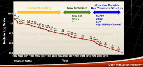
It took Morris 3 years to answer that question. By 1987, he had launched Taiwan Semiconductor Manufacturing Corporation (TSMC) – a company that manufactured chips for others, as a service. The company is known as a foundry because of the similarity of its business model with that of metal casting foundries in operation since early 19th centur

I never met Morris Chang. But, for the three decades that followed, I was his fellow traveler, a keen observer, a student, and a competitor.

Back in 1984, I was a 27 year old electronics engineer starting my career with Intel. Intel was (and still is) an Integrated Device Manufacturer (IDM). The IDM business model is the opposite of the foundry business model. An IDM develops manufacturing capability for its own products designed by its own IC designers. A foundry on the other hand, develops manufacturing capability for its customers’ products designed by its customers’ IC designers. A foundry helps its customers compete with IDMs.

Intel and TSMC grew up as leaders in the semiconductor industry they helped shape. Both drove exponentials: one in the electronics capability world-wide, and another in the reduction of cost for that capability. It resulted in fundamental changes in the way we live.

For most of this period, the industry generally accepted Intel as the leader at the edge of Moore’s Law, by at least a generation. I was one of the Intel voices shining light on Intel’s lead and explaining how that lead gives a competitive edge to Intel’s chips. Publicly, Morris did not indulge much in the technology leadership question, choosing instead to emphasize TSMC’s brand promise of customer service, trustworthiness and breadth of offerings.

In a 1998 interview, Morris said “The main thing that we’ve learned is that foundry is a service-oriented business, so we are molding ourselves into a service company”. These words were not from a business school slide. They came from deep and powerful insights of a master business man. They captured the pith of TSMC’s winning strategy. An important aspect of the service strategy was the harvesting of immense knowledge from the intimate teamwork between TSMC technologists and its customers’ IC designers. The willingness to learn from his customers was crucial in targeting and tuning his offerings to match his customers’ needs.

His emphasis on customer service did not mean TSMC was not focused on advancing with Moore’s Law. It was. I once described this pursuit as a group led by Intel, running towards an invisible wall, on an increasingly difficult terrain, and in a fog that was getting denser by the year. During this journey, Intel could hear the sounds of rival footsteps behind it, with many growing fainter over time. But not TSMC’s. It had been consistent, even getting louder, as it pulled up to Intel and started running shoulder to shoulder. Morris was clear about the importance of technology in making his customers competitive. In one interview he said “TSMC will stand behind our customers and cooperate with them. The battlefield between our customers and Intel is where we compete against Intel”.

The dawn of this century saw a change in client computing landscape. By then, the computer had spread from the desktop to the lap, but the move to the pocket was just starting. Intel assumed that Intel Architecture would sail into the pocket as easily as it did into the laptop. History however, proved that assumption wrong. The late Paul Otellini, Intel’s CEO at the time, considered that as one of his most significant failures. It was, in fact, Intel’s failure, not just his own. We at Intel felt entitled to success in markets where we were not incumbents. Our actions and inactions were rooted in that. But this was one of TSMC’s most spectacular successes, a result of years of customer-driven learning and delivering to commitments.

By 2008, Intel had launched a foundry division called Intel Custom Foundry (ICF), aiming to manufacture custom products for strategic customers. Intel was not the first to think of creating a foundry within an IDM. IBM offered foundry services long before that, and so did Samsung. However, due to Intel’s reputation as the leader in pursuit of Moore’s Law, even the most skeptical potential customers were intrigued, despite their concerns about incompatibility between the foundry and the IDM models. With ICF, Intel competed directly with TSMC. I led the formation and build up of ICF.

Soon, I came face to face with TSMC on the battlefield. In 2013, Altera Corp decided to switch from TSMC to Intel for their leading edge chips. Although Altera was not one of the highest revenue customers of TSMC, it was a strategic customer because it drove the leading edge of Moore’s Law. At the Q1 2013 TSMC earnings call, Morris was asked questions about the design loss of Altera. He said that he hates to lose even a part of an old customer. He said he regretted the loss and because of this, TSMC had investigated and thoroughly critiqued itself. He continued “..and there were, in fact, many reasons why it happened and we have taken them to heart. It’s a lesson to us and at least, we’ll try our very best not to let similar things happen again”. He clearly held himself accountable for the loss and resolved to do something about it. His humility was admirable and disarming. It kept me from gloating over my win.

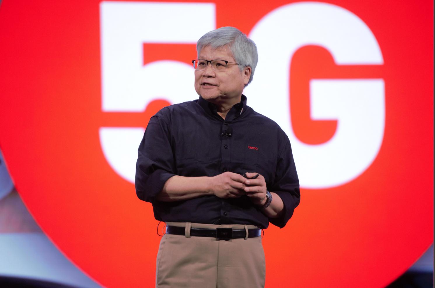
Morris Chang was 55 when he started TSMC, and he walked away earlier this month, ending his glorious innings at age 86. This transformational giant of the semiconductor industry taught us through his goal clarity, personal humility, and tenacious stamina, that inspiration can hit at any age, and spectacular climbs to unimagined peaks can be undertaken anytime. Thank you, Morris.


7nm, 5nm and 3nm Logic, current and projected processes

7nm, 5nm and 3nm Logic, current and projected processes
by Scotten Jones on 06-25-2018 at 7:00 am

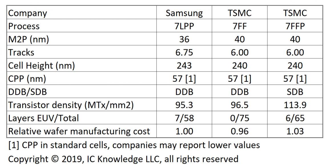
There has been a lot of new information available about the leading-edge logic processes lately. Papers from IEDM in December 2017, VLSIT this month, the TSMC and Samsung Foundry forums, etc. have all filled in a lot of information. In this article I will summarize what is currently known.
Continue reading “7nm, 5nm and 3nm Logic, current and projected processes”


TSMC OIP DAC Theater Schedule 2018

TSMC OIP DAC Theater Schedule 2018
by Daniel Nenni on 06-20-2018 at 6:00 am

The TSMC OIP DAC Theater schedule is finalized and ready to go. It kicks off Monday at 10:15 am in booth #1629 and ends with a raffle at 5:45 pm each day (Mon-Tue-Wed) TSMC gives out some very nice prizes so check in with the TSMC booth staff when you arrive. There are 66 coveted presentation spots representing the top ecosystem partners around the world. The TSMC theater is one of the busiest and if you look at the attached schedule you will see why.

TSMC OIP DAC:
Overview Schedule Raffle

Honorable mentions go to the presentations by companies that we work with:

  • Analog Bits: A Case Study of FinFet SERDES for AI
  • ANSYS: ADAS Reliability for Advanced FinFET Design
  • Cadence: Virtuoso Design Platform for Advanced Nodes
  • Cadence: Advanced Semiconductor Packaging
  • Cadence: IP Solutions for Advanced Nodes
  • Cadence: High Performance 7nm Digital Design
  • Flex Logix: Applications and Value Proposition of eFPGA by Market
  • Moortec: FinFET Optimization and Reliability Enhancement
  • Mentor: Verification Solutions for TSMC Advanced Packaging
  • Mentor: Verification and Advanced DRC
  • Mentor: Tessenet DFT Yield Solutions for Advanced Nodes
  • SiFive: Enabling Access to Silicon
  • Silicon Creations: High Performance PLL Design on 5nm FinFET
  • Silvaco: Technology Behind the Chip
  • Synopsys: Silicon Proven Designware IP for TSMC Processes
  • Synopsys: Power ECOs with ANSYS Redhawk
  • Synopsys: Custom Platform for TSMC
  • TSMC OIP Update

Special mention goes to Open Silicon who sent abstracts for their TSMC theater presentations:

Topic: Turnkey 2.5D HBM2 ASIC SiP Solution for Deep Learning and Networking Applications
Presenter: Asim Salim / VP of Manufacturing Operations, Open-Silicon

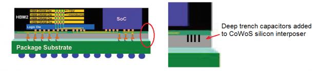
The most common memory requirements for emerging deep learning and networking applications are high bandwidth and density, based on real-time random operations. High Bandwidth Memory (HBM2) meets these requirements and delivers unprecedented bandwidth, power efficiency and small form factor. Open-Silicon’s silicon proven HBM2 IP subsystem in TSMC’s FinFET and CoWoS® technologies is enabling next generation high bandwidth applications and the successful ramping of 2.5D HBM2 ASIC SiP designs into volume production.

Topic:IP Subsystem solutions for Deep Learning and Networking Applications
Presenter: Kalpesh Sanghvi / Technical Manager of IP and Platforms, Open-Silicon

For Deep Learning and Networking applications ASICs, HBM IP Subsystem, Networking IP Subsystem are main building blocks. Open-Silicon’s first HBM2 IP subsystem in 16FF+ is silicon-proven at 2Gbps data rate, achieving bandwidths up to 256GBps. Open-Silicon’s next generation HBM2 IP subsystem supports 2.4Gbps in 16FFC, achieving bandwidths up to >300GBps and supports 3.2Gbps and beyond data rates in 7nm, achieving bandwidths up to >400GBps. Open-Silicon’s Networking IP subsystem includes high-speed chip-to-chip interface Interlaken IP, Ethernet Physical Coding Sublayer (PCS) IP, FlexE IP compliant to OIF Flex Ethernet standard v1.0 and v2.0, and Multi-Channel Multi-Rate Forward Error Correction (MCMR FEC) IP.

Topic:Package Design, Assembly and Test Strategies for Robust 2.5D HBM2 ASIC SiP Manufacturing
Presenter: Abu Eghan / Sr. Manager of Packaging & Assembly, Operations, Open-Silicon

2.5D HBM2 ASIC SiPs manufacturing has unique challenges for package design, assembly and testing both at the wafer level and the SiP level. Open-Silicon’s has proven solutions and strategies that are available to mitigate these issues in order to successfully ramp ASIC SiP designs into volume production.

About DAC
The Design Automation Conference (DAC) is recognized as the premier event for the design of electronic circuits and systems, and for electronic design automation (EDA) and silicon solutions. A diverse worldwide community representing more than 1,000 organizations attends each year, represented by system designers and architects, logic and circuit designers, validation engineers, CAD managers, senior managers and executives to researchers and academicians from leading universities. Close to 60 technical sessions selected by a committee of electronic design experts offer information on recent developments and trends, management practices and new products, methodologies and technologies. A highlight of DAC is its exhibition and suite area with approximately 200 of the leading and emerging EDA, silicon, intellectual property (IP) and design services providers. The conference is sponsored by the Association for Computing Machinery’s Special Interest Group on Design Automation (ACM SIGDA), the Electronic Systems Design Alliance (ESDA), and the Institute of Electrical and Electronics Engineer’s Council on Electronic Design Automation (IEEE CEDA).


Welcome DDR5 and Thanks to Cadence IP and Test Chip

Welcome DDR5 and Thanks to Cadence IP and Test Chip
by Eric Esteve on 05-25-2018 at 7:00 am

Will we see DDR5 memory (device) and memory controller (IP) in the near future? According with Cadence who has released the first test chip in the industry integrating DDR5 memory controller IP, fabricated in TSMC’s 7nm process and achieving a 4400 megatransfers per second (MT/sec) data rate, the answer is clearly YES !

Let’s come back to DDR5, in fact a preliminary version of the DDR5 standard being developed in JEDEC, and the memory controller achieving a 4400 megatransfers per second. This means that the DDR5 PHY IP is running at 4.4 Gb/s or quite close to 5 Gb/s, the speed achieved by the PCIe 2.0 PHY 10 years ago in 2008. At that time, it was the state of the art for a SerDes, even if engineering teams were already working to develop faster SerDes (8 Gb/s for SATA 3 and 10 G for Ethernet). Today, the DDR5 PHY will be integrated in multiple SoC, at the beginning in these targeting enterprise market, in servers, storage or data center applications.

These applications are known to always require more data bandwidth and larger memories. But we know that, in data center, the power consumption has become the #1 cost source leading to incredibly high electricity bill and more complex cooling systems. If you increase the data width for the memory controller while increasing the speed at the same time (the case with DDR5) but with no power optimization, you may come to an unmanageable system!
This is not the case with this new DDR5 protocol, as the energy per bit (pJ/b) has decreased. But the need for much higher bandwidth translates into larger data bus width (128-bit wide) and the net result is to keep the power consumption the same as it was for the previous protocol (DDR4). In summary: larger data bus x faster PHY is compensated by lower energy/bit to keep the power constant. The net result is higher bandwidth!

You have probably heard about other emerging memory interface protocols, like High Bandwidth Memory 2 (HBM2) or GraphicDDR5 (GDDR5) and may wonder why would the industry need another protocol like DDR5?
The answer is complexity, cost of ownership and wide adoption. It’s clear that all the DDRn protocols, as well as the LPDDRn, have been dominant and saw the largest adoption since their introduction. Why will DDR5 have the same future as a memory standard?

If you look at HBM2, this is a very smart protocol, as the data bus is incredibly wide, but keeping the clock rate pretty low (1024 bit wide bus gives 256 Gbyte/s B/W)… Except that you need to implement 2.5D Silicon technology, by the means of an interposer. This is a much more complex technology leading to much higher cost, due to the packaging overcost to build 2.5D, and also because of the lower production volume for the devices which theoretically lead to higher ASP.

GDDR5X (standardized in 2016 by JEDEC) targets a transfer rate of 10 to 14 Gbit/s per pin, which is clearly an higher speed than DDR5, but requires a re-engineering of the PCB compared with the other protocols. Sounds more complex and certainly more expansive. Last point, if HBM2 has been adopted for systems where the bandwidth need is such than you can afford an extra cost, GDDR5X is filling a gap between HBM2 and DDR5, this sounds like the definition of a niche market!

If your system allows you to avoid it, you shouldn’t select a protocol seen as a niche. Because the lower the adoption, the lower the production volume, and the lower the competition pressure on ASP device cost… the risk of paying higher price for the DRAM Megabyte is real.

If you have to integrate DDR5 in your system, most probably because your need for higher bandwidth is crucial, Cadence memory controller DDR5 IP will offer you two very important benefits: low risk and fast TTM. Considering that early adopters have already integrated Cadence IP in TSMC 7nm, the risk is becoming much lower. Marketing a system faster than your competitors is clearly a strong advantage and Cadence is offering this TTM benefit. Last point, Cadence memory controller IP has been designed to offer high configurability, to stick with your application needs.

From Eric Esteve (IPnest)

For more information, please visit: www.cadence.com/go/ddr5iptestchip.


TSMC Technologies for IoT and Automotive

TSMC Technologies for IoT and Automotive
by Alex Tan on 05-15-2018 at 12:00 pm

At TSMC 2018 Silcon Valley Technology Symposium, Dr Kevin Zhang, TSMC VP of Business Development covered technology updates for IoT platform. The three growth drivers in this segment namely TSMC low power, RF enhancement and embedded memory technology (MRAM/RRAM) reinforced both progress and growth in global semiconductor revenue since 1980 –from PC, notebook, mobile phone, smartphone and eventually IoT. For 2017-2022 period, CAGR of 24% and 6.2B units of IoT end devices shipment by 2022 are projected.
Continue reading “TSMC Technologies for IoT and Automotive”


TSMC Technologies for Mobile and HPC

TSMC Technologies for Mobile and HPC
by Alex Tan on 05-10-2018 at 12:00 pm

During TSMC 2018 Technology Symposium, Dr. B.J. Woo, TSMC VP of Business Development presented market trends in the area of mobile applications and HPC computing as well as shared TSMC progress in making breakthrough efforts in the technology offerings to serve these two market segments.

Both 5G and AI are taking the center stage in shaping the high double-digit data growth demand. For mobile segment, the move from 4G LTE to 5G requires the use of higher modem speed (from 1Gbps to 10Gbps), 50% faster CPU, twice faster GPU, double transistor density, 3X performance increase of AI engines to 3 TOPS (Trillion Operations Per Seconds) target and without much power increase. In this market segment, TSMC is ushering the move from 28HPC+ towards 16FFC.

On the cloud side, data center switch demands double throughput, from 12.8Tbps to 25.6Tbps as the computing demand move towards the network edge. Similarly the drive towards double memory bandwidth, 3 to 4x increase in throughput of AI accelerators and up to 4x transistor density improvement are taking place.

N7 Technology Progress
Dr. Woo stated that delivering high density and power efficiency requirements to satisfy low latency of data intensive AI application is key to the success of TSMC N10 process. It has also enabled AI in the smartphones space. On the sideline, N7 node has been making good progress in providing excellent PPA values with >3x density improvement, >35% speed gain and >65% power reduction over its 16nm predecessor.

N7 HPC track provides 13% speed over N7 mobile (7.5T vs 6T), while it has passed the yield and qual tests (SRAM, FEOL, MEOL, BEOL) and MP-ready D0. Part of the contributing factor is TSMC successful leveraged learning from N10 D0 and it is targeted for Fab15.

The N7 IP ecosystem is also in ready state with over 50 tapeouts slated by end of 2018 for mobile, HPC, automotive and servers. The 7nm technology is anticipated to be having a long life similar to its predecessor 28nm/16nm nodes. The combination of mild pitch scaling from N10 to N7 plus the migration from immersion to EUV scaling and denser standard cell architecture make significant overall improvement.

EUV Adoption and N7+ Process Node
She shared some progress of the EUV application on N7+. Applicable on selected layers, EUV reduces the process complexity and enhances resulting pattern fidelity. It also enables future technology scaling while offering better performance, yield and shorter cycle time. Dr. Woo showed caption of via resistance having much tighter distribution in N7+ EUV versus N7+ immersion as it delivers better uniformity.

The N7+ value proposition includes delivering 20% more logic density over N7, 10% lower power at same speed, and additional performance improvements anticipated from the ongoing collaboration with customers.

N7+ will also have double digit good die increase over N7 node as it gains traction from capitalizing the use of the same equipment and tooling. She claimed that it has lower defect density than other foundries as well as comparable 256Mb SRAM yield and device performance vs N7 baseline. TSMC provides easy IP porting (layout and re-K) from N7 to N7+ for those design entities that do not need to be redesigned.

HPC and N7+ Process Node
For HPC platform solution, the move from N7 to N7+ involves the incorporation of EUV, denser standard cell architecture, ultra-low Vt transistors, high-performance cells, SHDMIM (Super High Density MIM) capacitance and larger CPP (Contacted Poly Pitch) and 1-fin cells.

N7+ offers better performance and power usage through the use of an innovative standard cell architecture. It allows higher fin density in the same footprint for 3% speedup. On the other hand, reducing power by applying single-fin in non-timing-critical area reduces about 20% capacitance and in-turns, the dynamic power number.

The adoption of new structures also enhances MIM capacitance and utilization rate for HPC 3% to 5% performance boost. N7+ design kit is ready for supporting the IP ecosystem.

N5 Value Proposition
It has new elVt (extreme low Vt) offering a 25% max speed-up versus N7, incorporating aggressive scaling and full-fledged EUV. N5 has made good progress with double digit yield on 256Mb SRAM. Risk production is slated to be 1H2019.

Dr. Woo also shared a few metrics compared with N7 process (test vehicles used ARM A72 CPU core + internal ring oscillator):
– 15% speed improvement (up to 25% max speed)
– 30% power reduction
– 1.8x increased logic density through innovative layout and routing
– 1.3x analog density improvement through poly pitch shrink and selective Lg and fin #, yielding a more structured layout (“brick-like” patterns)

16FFC/12FFC Technologies
Dr. Woo covered RF technologies and roadmap (more on this in subsequent blog on IoT and Automotive). She mentioned that N16 and N12 FinFet based platform technologies have broad coverage, addressing HPC, mobile, consumer and automotive. Both 16FFC and 12FFC have shown strong adoption data with over 220 tapeouts. 12FFC should deliver 10% speed gain, 20% power reduction and 20% increased logic density vs 16FFC through dual-pitch BEOL, device boost, 6-track stdcell library and 0.5v VCCmin.

To recap, AI and 5G are key drivers for both mobile and HPC product evolutions. Along this line, TSMC keeps pushing the PPA (Power, Performance and Area) envelopes for the mainstream products while delivering leading RF technologies to keep pace with technology accelerated designs in these segments.

Also read: Top 10 Highlights of the TSMC 2018 Technology Symposium


Top 10 Highlights of the TSMC 2018 Technology Symposium

Top 10 Highlights of the TSMC 2018 Technology Symposium
by Tom Dillinger on 05-04-2018 at 12:00 pm

Here are the Top 10 highlights from the recent TSMC 2018 Technology Symposium, held in Santa Clara CA. A couple of years ago, TSMC acknowledged the unique requirements of 4 different market segments, which has since guided their process development strategy — Mobile, High-Performance Computing (HPC), Automotive, and IoT. Many of the highlights described below are in the context of a specific platform.
Continue reading “Top 10 Highlights of the TSMC 2018 Technology Symposium”


Leading Edge Logic Landscape 2018

Leading Edge Logic Landscape 2018
by Scotten Jones on 03-16-2018 at 2:00 pm

The most viewed blogs I write for SemiWiki are consistently blogs comparing the four leading edge logic producers, GLOBALFOUNDRIES (GF), Intel, Samsung (SS) and TSMC. Since the last time I compared the leading edge new data has become available and several new processes have been introduced. In this blog I will update the current status.
Continue reading “Leading Edge Logic Landscape 2018”


Webinar: Multiphysics Reliability Signoff for Next-Generation Automotive Electronics Systems

Webinar: Multiphysics Reliability Signoff for Next-Generation Automotive Electronics Systems
by Bernard Murphy on 02-08-2018 at 7:00 am

In case you missed the TSMC event, ANSYS and TSMC are going to reprise a very important topic – signing-off reliability for ADAS and semi-autonomous /autonomous systems. This topic hasn’t had a lot of media attention amid the glamor and glitz of what might be possible in driverless cars. But it now seems like the cold light of real engineering needs are advancing over the hype, if this year’s CES is any indication (see my previous blog on CES). Part of that engineering reality is ensuring not only that we can build these clever systems but that they will also continue to work for a respectable amount of time; in other words that they will be reliable, a topic as relevant for today’s advanced automotive electronics as it is for the systems of tomorrow.

REGISTER HERE for this event on February 22nd at 8am Pacific Time

This topic is becoming a pressing concern, especially for FinFET-based designs. There are multiple issues impacting aging, stress and other factors. Just one root-cause should by now be well-known – the self-heating problem in FinFET devices. In planar devices, heat generated inside a transistor can escape largely through the substrate. But in a FinFET, dielectric is wrapped around the fin structure and, since dielectrics generally are poor thermal conductors, heat can’t as easily escape leading to a local temperature increase, and will ultimately escape significantly through local interconnect leading to additional heating in that interconnect. Add to that increased Joule heating thanks to higher drive and thinner interconnect and you can see why reliability becomes important.

ANSYS has developed an amazingly comprehensive range of solutions for design for reliability, spanning thermal, EM, ESD, EMC, stress and aging concerns. In building solutions like this, they work very closely with TSMC, so much so that they got three partner of the year awards at the most recent TSMC OIP conference!

Incidentally my CES-related blog is here: https://www.legacy.semiwiki.com/forum/content/7274-ces-exhibitor-s-takeaway.html

Summary
Design for reliability is a key consideration for the successful use of next-generation systems-on-chip (SoCs) in ADAS, infotainment and other critical automotive electronics systems. The SoCs manufactured with TSMC’s 16FFC process are advanced multicore designs with significantly higher levels of integration, functionality and operating speed. These SoCs must meet the rigorous requirements for automotive electronics functional safety and reliability.

Working together, ANSYS and TSMC have defined workflows that enable electromigration, thermal and ESD verification and signoff across the design chain (IP to SoC to package to system). Within the comprehensive workflows, multiphysics simulations capture the various failure mechanisms and provide signoff confidence not only to guarantee first-time product success, but also to ensure regulatory compliance.

Attend this ANSYS and TSMC webinar to learn about ANSYS’ chip-package-system reliability signoff solutions for creating robust and reliable electronics systems for next-generation automotive applications, and to explore case studies based on TSMC’s N16FFC technology.

Founded in 1970, ANSYS employs nearly 3,000 professionals, many of whom are expert M.S. and Ph.D.-level engineers in finite element analysis, computational fluid dynamics, electronics, semiconductors, embedded software and design optimization. Our exceptional staff is passionate about pushing the limits of world-class simulation technology so our customers can turn their design concepts into successful, innovative products faster and at lower cost. As a measure of our success in attaining these goals, ANSYS has been recognized as one of the world’s most innovative companies by prestigious publications such as Bloomberg Businessweek and FORTUNE magazines.

For more information, view the ANSYS corporate brochure.


Machine Learning And Design Into 2018 – A Quick Recap

Machine Learning And Design Into 2018 – A Quick Recap
by Alex Tan on 02-07-2018 at 3:00 pm

How could we differentiate between deep learning and machine learning as there are many ways of describing them? A simple definition of these software terms can be found here. Let’s look into Artificial Intelligence (AI), which was coined back in 1956. The term AI can be defined as human intelligence exhibited by machines. While machine learning is an approach to achieve AI and deep learning is a technique for implementing subset of machine learning.


During last year 30-Year Anniversary of TSMC Forum, nVidia CEO Jen-Hsen Huang mentioned two concurrent dynamics disrupting the computer industry today, i.e.,how software development is done by means of deep learning and how computing is done through the more adoption of GPU as replacement to single-threaded/multi-core CPU, which is no longer scale and satisfy the current increased computing needs. The following charts illustrate his message.


At this month Santa Clara DesignCon2018 there were multiple well-attended sessions (2 panels and 1workshop) addressing Machine Learning Advances in Electronic Design. Highlighted by panelists coming from 3 different areas (EDA, industry and academia) were some successful snapshots of ML application in optimizing design and its potential consequences as how we should handle the generated models and methodologies.

From the industry:
Chris Cheng, a Distinguished Engineer from HPE presented a more holistic view of ML potential use coupled with test instruments as substitute for a software model based channel analysis. He also projected ML use to perform more proactive failure prediction of signal buses or complicated hardware such as solid-state drives.


Ken Wu, Google Staff HW Engineer shared his works on applying ML in channel modeling. He proposed the use of ML to predict channel’s eye-diagram metrics for signal integrity analysis. The learned models can be used to circumvent the need of performing complex and expensive circuit simulations. He believes ML opens an array of opportunity for channel modeling such as extending it to analyze the four-level pulse amplitude modulation (PAM-4) signaling, and the use of Deep Neural Network for Design of Experiment (DOE).

Dale Becker, IBM Chief Engineer of Electronic Packaging Integration, alluded to the potential dilemma imposed by ML. Does it supersede today’s circuit/channel simulation techniques, or is it synergistic? With the current design methodologies still reflecting heavy human interventions (such as in channel diagnostics, evaluation, optimization, physical implementation), ML presents an opportunity for exploration. On the other side of the equation, we need to be ready to address standardization, information sharing and IP protection.

From the EDA world, both Synopsys and Cadence were represented:

Cadence team — David White (Sr. Group Director), Kumar Keshavan (Sr. Software Architect) and Ken Willis (Product Engineering Architect) highlighted Cadence contribution in advancing ML adoption. David shared what Cadence has achieved with ML over the years on Virtuoso product and raised the crucial challenge of productizing ML. For a more in-depth coverage for David’s similar presentation on ML, please refer to another Wiki article TSMC EDA 2.0 With Machine Learning – Are We There Yet ? Kumar delved into Artificial Neural Network (ANN) concept and suggested its application for DOE of LPDDR4 bus. Ken Willis was moderating the afternoon panel and highlighted the recently introduced IBIS ML versus AMI model as well as impact of ML on solution space analysis.


Sashi Obilisetty, Synopsys R&D Director pointed out that the EDA ecosystem comprising of academic research, technology availability and industry interest) is ready and engaged. What we need is a robust, scalable, hi-performance and near real time data platform for ML application.

Several academia also shared their research progress under the auspice of Center for Advanced Electronics Through Machine Learning (CAEML) since its formation in 2016:

Prof. PaulFranzon discussed how ML could shorten IC physical design step through the use of surrogate model. The concept is to train a fast global model to evaluate from multiple evaluations of a detailed model that is slow to evaluate. Given an SOC design requiring a 40 minute per route iteration, the team needs about 50 runs to complete the Kriging based model overnight. Using this model, an optimal design can be obtained in 4 iterations which otherwise requires 20 iterations. The design has 18K gates derived from Cortex-M0 with 10ns cycle time and 45nm generic process.

Prof. Madhavan Swaminathan presented another application of ML based solution using surrogate model on channel performance simulation.

His view: Engineer (thinker) + ML (enabler) + Computers (doers) = enhanced solution. Extending ML into design optimization through active learning may ensure convergence to global optima and minimizing required CPU time.

With the increased design activities and research efforts in ML/DL applications, we should anticipate more coverage of such implementation into 2018. The next question would be if it will create a synergy and enhance design efforts through retooling and methodology adjustments, or it will create disruption that may change the human designer roles at different junctures of design capture. We should see.