Apple’s recent Spring Loaded Event brought us M1-based iMacs. After the MacBook Air and 13” MacBook Pro in the fall, iMacs are the third Mac to jettison Intel processors. With this transition Apple’s T2 chip enters End of Life status, so to speak. The T2 is a bit of an enigma and now it does not have much time left.
We know it performs a wide range of tasks in Macs, including security, encryption, video processing, storage control and housekeeping. This 2019 AppleInsider article tested encode times for Macs having the same processor, where one had a T2, and one did not. The Mac with the T2 executed the encode in 1/2 the time.
Despite all this functionality we know surprising little about the T2. There simply is not much information floating around. Wikipedia does not even report a die size or process node. Did Apple design a whole new chip? How much is borrowed from the A-series family? How much is new design? How much is Apple investing to achieve the desired functionality for Macs? It is time to look at a T2 and find out what Apple created for their Intel-based Mac co-processor.
Package & hints of memory
The T2 under study came from a 2019 13” MacBook Air logic board. The T2’s package has a decent footprint compared to the other ICs around it. For comparison, the larger of the shiny dies to the right of the T2, between four mounts, is the Intel i5. One can envision the T2 being a similar size, based on the package. There is a “1847” date code on the package indicating late 2018 assembly.
2019 13” MacBook Air logic board
A teardown of the late 2018 MacBook Air simply listed the T2’s part number. However, a teardown of a 2019 15” MacBook Pro indicated the T2 was “layered on a 1 GB Micron D9VLN LPDDR4 memory”. Our package also included the “D9VLN” marking. A decoder at Micron points to a 1GB LPDDR4. The T2 and memory would likely be in a Package-On-Package (PoP) arrangement.
A second die was in fact found in the beaker after de-packaging. The markings visible at top metal are Micron’s. The inclusion of in-package DRAM is interesting, not to mention costly, for a companion IC or co-processor. It is however not too surprising considering the T2 is derived from the A-series that has long had in-package DRAM.
Top metal die markings of second die in T2 package.
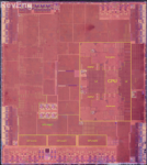
Die photo & “PUs”
It is time for the main event. SEM analysis of several line pitches and 6T SRAM cell size confirmed the T2 is fabbed in a TSMC16 nm process. This is the same node as the A10, so the latter will serve as a reference A-series processor against which the T2 can be compared.
T2 die photo with CPU and GPU annotations.
A10 die photo with original annotations. Source: Chipworks
Visually, the CPU is the first thing that jumps out at you. It is the same design and layout as the A10. Assuming the T2 was designed after the A10, the CPU was dropped in as a hard macro. Remember it is a 4-core CPU! There are two performance i.e. large Hurricane cores and two efficiency i.e. small Zephyr cores. That is quite a bit power considering there is already an Intel i5 for the main system processor.
One can only imagine the conversation within Apple. “Do you have any CPU’s ready to go?” “Yup … there is a 4-core 17.4 mm2 design that is only a few months old on the shelf over there.” “Great, I’ll take one of those.” Well, maybe it was a bit more technical.
The GPU does not follow suit. The A10’s 6-core GPU is organized as 3 blocks for the cores and a block of logic. The T2’s GPU appears to be along the lower edge of the die. Again, the cores are organized as 3 blocks. We did not discern symmetry within these blocks, suggesting 3 cores. The GPU logic is likely in a block just above the cores, where the hashed lines encircle a potential area for it. Even if all 3 blocks within this area were GPU logic, it would be smaller than that identified for the A10. There is more analysis needed here to confirm the GPU configuration, but there are suggestions that both the GPU’s logic and cores are smaller than those on the A10.
Additional block-level analysis is ongoing. We see blocks that were used as-is, when compared to the A10, ones that received a new layout, and straight-up new design.
Early numbers
The T2 measures 9.6 mm by 10.8 mm, yielding a die size of 104 mm2. It is not a small die! The T2 is a serious processor. This is roughly 80% of the A10’s 125 mm2.
As expected, the CPU has an area of approximately 17.4 mm2 on both dies. This yields a higher % of the total die dedicated to the CPU in the T2. The T2’s GPU is considerably smaller than the A10’s. Each core comes in at 1.2 mm2 v. 5.3 mm2 for the cores of the A10. Functionally, this makes sense as the T2 GPU should not be tasked near as much as the A10’s because it is not the primary GPU. Again, there is already either Intel embedded graphics or a dedicated GPU on the logic board.
Pulling threads together
There is plenty more to extract from the reverse engineering, but this snippet provides a flavor of Apple’s thinking. As a starting point, Apple looks to user functionality. An ongoing question at Apple seems to be “What do we want the user to experience from an Apple product?” Then they build it. The T2 became Apple’s interpretation of this for Intel-based Macs, but remember prior to the T1 the Intel processors were flying solo, and Macs still worked.
The T2 leveraged design from the A-series processors as shown in the CPU. It’s 4-core CPU is large, to say the least, and it is hard not to think it is overpowered for the T2. That said, Apple would look at the cost of re-design v. the silicon cost associated with dropping in something that might be larger than is truly needed. The latter was probably more enticing as the wafer starts for the T2 would be nowhere near those of the A10, or any A-series processor for that matter. Besides, the extra horsepower will provide a better experience.
The T2 also consolidated stand-alone ICs within a Mac. The storage or SSD controller is one example of this. Apple bought Israeli-based Anobit in 2011. The 2016 13” MacBook Pro (with Function Keys) included an Apple stand-alone storage controller (see slide 11). The controller became a block on the T2. Today, it would be a block on the M1.
Conclusion
We will continue to dig into the T2, focusing on the known block functionalities, it’s comparison with the A10 and looking forward. Yes, the T2 and the A10 are both old designs, but the comparison liberates information about use of semiconductor design and the effort Apple invests to provide their desired user experience.
*This article is jointly authored by Lev Klibanov. Dr. Klibanov is an independent consultant in semiconductor process and related fields. Dr. Klibanov has focused on and has considerable experience in advanced CMOS logic, non-volatile memory, CMOS image sensors, advanced packaging, and MEMS technologies. He has spent 20+ years working in reverse engineering, metrology, and fabrication.