TSMC recently held their 10th annual Open Innovation Platform (OIP) Ecosystem Forum. An earlier article summarized the highlights of the keynote presentation from L.C. Lu, TSMC Fellow and Vice-President, Design and Technology Platform, entitled “TSMC and Its Ecosystem for Innovation” (link).
Overview of 3D Fabric
The TSMC 3D Fabric advanced packaging technology spans both the 2.5D and vertical die stacking offerings, as depicted below.
The Integrated FanOut (InFO) packages utilize a reconstituted wafer consisting of die embedded face down, surrounded by a molding compound (link).
Redistribution interconnect layers (RDL) are fabricated on the epoxy wafer. (InFO-L refers to a silicon “bridge chiplet” between die embedded in the InFO package for improved inter-die connectivity over the RDL metallization pitch.)
The 2.5D CoWoS technology integrates die (and often, high-bandwidth memory stacks) on an interposer utilizing microbump attach. The original CoWoS technology offering (now CoWoS-S) used a silicon interposer, and related silicon-based lithography for RDL fabrication; through-silicon vias (TSVs) provide connectivity to the package bumps. The silicon interposer technology offers improved interconnect density, critical for the high signal count HBM interface. More recently, TSMC has been offering an organic interposer (CoWoS-R), providing a tradeoff between interconnect density versus cost.
The 3D SoIC offering provides vertical integration utilizing hybrid bonding between die pads. The die may be oriented in face-to-face or face-to-back configurations. TSVs provide connectivity through the (thinned) die.
InFO and CoWoS offerings have been in high-volume production for several years. The recent innovations in CoWoS development relate to expanding the maximum silicon interposer dimensions to greater than the maximum reticle size to accommodate a larger number of die (especially, HBM stacks), stitching together the RDL interconnects.
The majority of Jim’s presentation covered advanced in SoIC development.
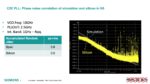
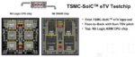
SoIC Testchip
TSMC shared results of a recent SoIC qualification test vehicle, as shown below.
The configuration used was the vertical bonding of an (N5) CPU die with an (N6) SRAM die, in a face-to-back topology. (Indeed, a major CPU vendor has pre-announced plans for a vertical “last-level” SRAM cache die attached to a CPU using TSMC’s SoIC, to be available in 1Q2022.)
SoIC Design Flow
Jim presented a high-level design flow for vertical die integration, as shown in the figure below.
The flow requires concurrent focus on both top-down system partitioning into individual die implementations, plus early analysis of the thermal heat dissipation in the composite configuration, as highlighted above.
The discussion on thermal analysis highlighted the “chimney” nature of the low thermal resistance paths of the BEOL PDN and interconnect, compared to the surrounding dielectrics, as shown above. Specifically, TSMC has collaborated with EDA vendors on improving the accuracy of the SoIC model discretization techniques, applying a more detailed mesh in specific “hotspot” areas initially identified with a coarse grid analysis.
TSMC also presented a methodology recommendation to incorporate thermal analysis results into the calculation of SoIC static timing analysis derate factors. Much like on-chip variation (OCV) is dependent upon the distance spanned by (clock and data) timing paths, the thermal gradient for the SoIC paths is an additional derate factor. TSMC reported that on-die temperature gradients for a path are typically ~5-10C, and a small flat derate timing margin for temperature should suffice. For SoIC paths, large gradients of ~20-30C are feasible. A flat derate to cover this range would be too pessimistic for paths with a small temperature difference – results of SoIC thermal analysis should be used for derate factor calculation.
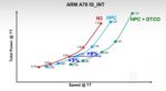
SoIC Testing
The IEEE 1838 standardization effort pertains to the definition of die-to-die interface testing (link).
Much like the IEEE 1149 standard for boundary-scan chains on-die for package-to-package testing on a printed circuit board, this standard defines the control and data signal ports on each die for post-stack testing. The primary focus of the standard is to exercise the validity of the face-to-face bonds and TSVs introduced during SoIC assembly.
Jim indicated that this definition is sufficient for low-speed I/Os between SoIC die, yet a more extensive BIST method will be required for high-speed I/O interfaces.
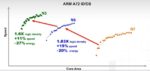
TSMC Foundation IP for SoIC – LiteIO
TSMC’s library development teams commonly provide general-purpose I/O cells (GPIOs) for each silicon process node. For the die-to-die connections in SoIC configurations, where the driver loading is less, TSMC offers a “LiteIO” design. As illustrated below, the LiteIO design focuses on optimizing the layout to reduce parasitic ESD and antenna capacitances, to enable faster datarates between die.
EDA Enablement
The figure below lists the key tool features recently developed in collaboration with major EDA vendors for the InFO and SoIC package technologies.
Summary
TSMC continues to invest heavily in 2.5D/3D advanced packaging technology development. The key recent initiatives have focused on the methodology for 3D SoIC direct die attach – i.e., partitioning, physical design, analysis. Specifically, early thermal analysis is a mandatory step. Additionally, TSMC shared results of their SoIC eTV qualification testchip vehicle. 2022 is shaping up to see the rapid emergence of 3D SoIC designs.
-chipguy
Also read:
Highlights of the TSMC Open Innovation Platform Ecosystem Forum
Highlights of the TSMC Open Innovation Platform Ecosystem Forum