Up until November of 2022, IC Knowledge LLC was an independent company and had become the world leader in cost and price modeling of semiconductors. In November 2022 TechInsights acquired IC Knowledge LLC and IC Knowledge LLC is now a TechInsights company.
For many years, IC Knowledge has published a database tracking all the 300mm wafer fabs in the world. Compiled from a variety of public and private sources, we believe the 300mm Watch database is the most detailed database of 300mm wafer fabs available. IC Knowledge LLC also produces the Strategic Cost and Price Model that provides detailed cost and price modeling for 300mm wafer fabs as well as detailed equipment and materials requirements. The ability to utilize both products to analyze a company provides a uniquely comprehensive view and we recently utilized these capabilities to do a detailed analysis of TSMC’s 300mm wafer fabs.
One way we check the modeling results of the Strategic Cost and Price Model is to compare the modeled spending on 300mm fabs for TSMC to their reported spending. Since the early 2000s nearly all of TSMC’s capital spending has been on 300mm wafer fabs and the Strategic Model covers every TSMC 300mm wafer fab.
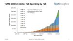
Figure 1 presents an analysis of TSMC’s cumulative capital spending by wafer fab site from 2000 to 2023 and compares it to the reported TSMC capital spending.
Figure 1. TSMC Wafer Fab Spending by Fab.
In figure 1 there is a cumulative area plot by wafer fab calculated using the Strategic Cost and Price Model – 2023 – revision 01 – unreleased, and a set of bars representing TSMC’s reported capital spending. One key thing to note about this plot is the Strategic Cost and Price Model is a cost and price model and fabs don’t depreciate until they are put on-line, therefore the calculated spending from the model is for when the fabs come on-line whereas the reported TSMC spending is when the expenditure is made regardless of when it comes on-line. TSMC’s capital spending also includes some 200mm fab, and mask and packaging spending. The TSMC reported spending is adjusted as follows:
- In the early 2000s estimated 200mm spending is subtracted from the totals. In some cases, TSMC announced what portion of capital spending was 200mm. In the overall cumulative total through 2022 this is a not a material amount of spending.
- Recently roughly 10% of TSMC’s capital spending is for masks and packaging, TSMC discloses this and it is subtracted from the total.
- When capital equipment is acquired but not yet put on-line, it is accounted for as assets in progress and this number is disclosed in financial filings. We subtract this number from the reported spending because the Strategic Model calculates on-line capital.
Note that fabs 12 and 20 are/will be in Hsinchu – Taiwan, Fabs 14 and 18 are in Tainan – Taiwan, Fab 15 is in Taichung – Taiwan, Fab 16 is in Nanjing – China, Fab 21 is in Arizona – United States, Fab 22 is planned for Kaohsiung – Taiwan and Fab 23 is being built in Kumamoto – Japan.
Some interesting conclusions from this analysis:
TSMC has spent roughly $135 billion dollars on 300mm wafers fabs through 2022. This number should break $200 billion dollars in 2024.
Fab 18 is TSMC’s most expensive fab (5nm and 3nm production), we expect that site to exceed $100 billion dollars in investment next year. Interestingly Fab 18 is right next to Fab 14 where an investment of more than $30 billion dollars has taken place and the combination next year will approach $140 billion dollars!
The capital investment of roughly $135 billion dollars in 300mm fabs just by TSMC is an amazing number, perhaps even more amazing is the investment is accelerating, should break $200 billion dollars in 2024 and could break $400 billion dollars by 2030.
Customers that license our 300mm Watch channel not only get the 300mm watch database along with regular updates, they also get access to this recent TSMC analysis and will also get access to a similar analysis we are doing of Samsung. For information on the 300mm Watch database or Strategic Cost and Price Model please contact sales@techinsights.com
Also Read:
SPIE Advanced Lithography Conference 2023 – AMAT Sculpta® Announcement


