The imec technology forum was held in Belgium last week. At the forum I had a chance to sit down with Gary Patton the CTO of GLOBALFOUNDRIES (GF) for an interview and he also presented “Enabling Connected Intelligence – Technology innovation: Enablers for an intelligent future” at the forum. In this article I will discuss what I see as the keys points from the presentation and interview.
Market opportunity
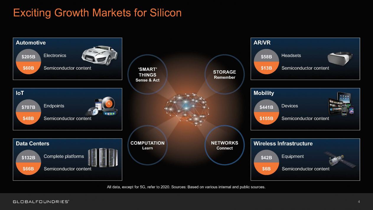
With the mobile market maturing there has been some concern that the industry will slow down. Gary presented a slide outlining the opportunities in Automotive, IoT, Data Centers, AR/VR, Mobility and Wireless Infrastructure with all six expected to double by 2020. Figure 1 illustrates the slide with the revenue opportunity at a product level and the semiconductor content forecast for 2020.

Figure 1. Exciting Growth Markets for Silicon.
Gary believes 5G will be even more disruptive than data was to voice in the mobile market. With IoT devices gathering data and transmitting it wirelessly up to the cloud, you will be able to do intelligent things with the data in the cloud.
Dual Roadmap
GF is committed to a dual track roadmap. For FinFETs GF has 14LPP, the new 12LPP (a mid life kicker for 14LPP) and 7LP ramping later this year. The second track is FDSOI with 22FDX in production now and 12FDX in development for release when the customers need it (more on this in the FDSOI section).
In my interview with Gary he noted that GF had achieved 80 tape-outs first time right.
FinFET
If you are developing large chips with high wire capacitance then FinFETs are the best solution.
GF offers 14LPP with high performance and balanced costs. GF also offers 12LP qualified in the Q1 2018 with 15% greater density than 14LPP, 0.5 volt operation for low power, >2.5GHz capability and >8.5M gates/mm2. AMD has announced they are producing processors on 12LP.
7LP will ramp later this year with ~50% area scaling versus 14LPP and >17M gates/mm[SUP]2[/SUP]. AMD and IBM are key 7nm customers and the 7FX program provides custom ASICs on 7nm, Gary noted that ASICs provide a good entry point for customers. First customer tape-outs are due in the second half with additional customer tape-outs in 2019. The Malta fab is now completely full and GF has more demand on 7nm than they can meet! Gary said he feels really good about where they are on 7LP, they don’t have the smallest pitches, but they are as dense as anyone. Authors note, my estimates are that GF 7LP is 98.21 MT/mm[SUP]2[/SUP], Samsung 7LPP is 95.30 MTx/mm[SUP]2[/SUP] and TSMC 96.49 MTx/mm[SUP]2[/SUP].
GF has two EUV tools installed in their Malta fab and will introduce EUV as soon as “it is ready”.
FD-SOI
FD-SOI is the second track of GFs roadmap.
22FDX is GF’s 22nm FD-SOI process and has 40% fewer masks than FinFETs, lower die cost, lower power and superior RF. For IoT, automotive and some mobile applications 22FDX is ideal. 22FDX offers 0.4 volt operation for low power, 1pA/µm leakage, >400GHz operation, embedded MRAM memory and the ability to integrate reasonable amounts of digital logic with analog and RF. GF is seeing a lot of RF designs on 22FDX.
The FD-SOI ecosystem had 7 partners in 2016, has 47 partners now and they expect to have 75 partners by the end of 2018. A robust design ecosystem is essential to the success of any technology and GF has made ecosystem development a focus. Gary did note they needed to do a little more on body bias since that is new concept for many customers.
22FDX yields are reported to be as good as GF’s 28nm bulk process yields.
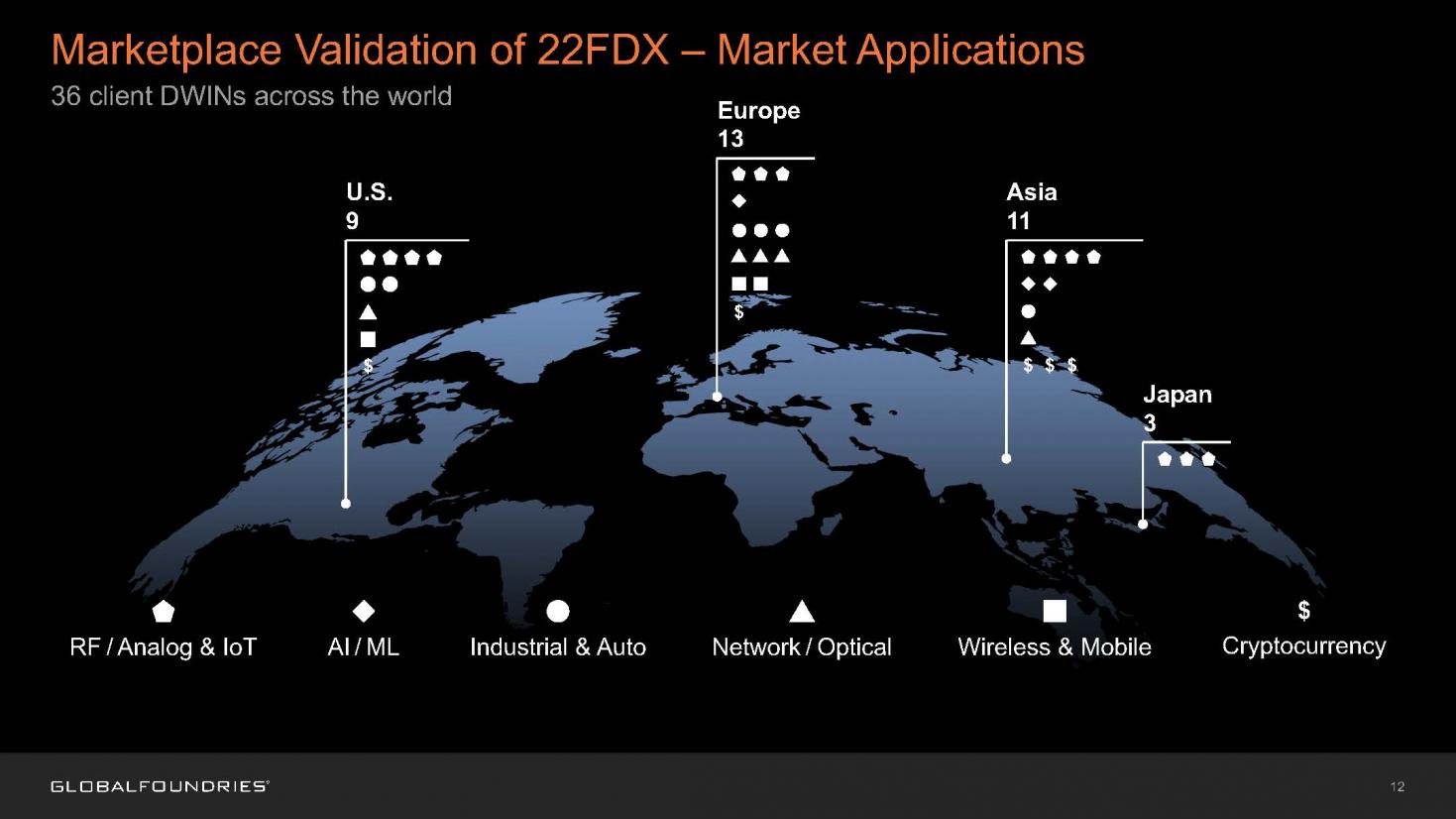
GF has 36 design wins for 22FDX across six different market segments around the world, see figure 2.

Figure 2. Market Validation of 22FDX – Market Applications.
Authors note, I get asked a lot whether I think FD-SOI is for real, I believe it is and that the preceding slide illustrates the growing market success for the technology.
22FDX is produced in GF’s Dresden fab and when that fab is full will also be produced in their new Chengdu fab. The Dresden fab became automotive qualified in Q1 of 2018.
As a follow-on to 22FDX, GF has 12FDX in development with full node scaling. I asked Gary about the status of 12FDX, he noted that customers are just now taping out on 22FDX and so they are focusing on 22FDX and 7LP and not really pushing on 12FDX but he said although early in development it is “fairly mature”.
5nm or 3nm
Tom Caufield, GF’s new CEO recently commented that GF is looking for partners for their next fab and that he thought 5nm might not be enough and they would have to go to 3nm.
I asked Gary about this.
Gary said assigning a node number would be up to marketing but that the next node after 7LP will be a full node scaling and a new architecture.
Authors note, based on full node scaling (~2.0x) from 7LP and new architecture (I would expect horizontal nanosheets) I expect this process to be similar to 3nm processes due from Samsung in 2021 and TSMC.
Conclusion
GF is executing well on their technical roadmap. They have a competitive 7nm FinFET offering and what I would characterize as the leading FD-SOI technology in the world.


Captain America: Can Elon Musk Save America’s Chip Manufacturing Industry?