Summary
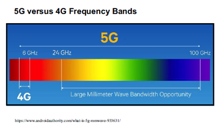
A recent process enhancement in advanced nodes is to support the fabrication of contacts directly on the active gate area of a device. At the recent VLSI 2020 Symposium, the critical advantages of this capability were highlighted, specifically in the context of the behavior of RF CMOS devices needed for 5G designs.
Introduction
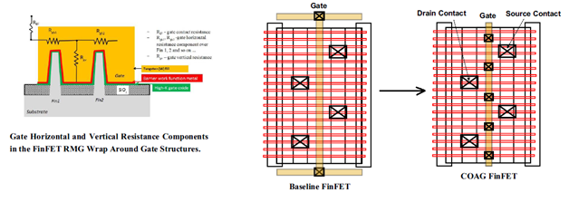
As shown in the left-hand figure below, the “conventional” layout design method is to place the contact for a logic gate input in the area between the (nMOS and pMOS) devices, leveraging the common connection between the two devices in a CMOS circuit. For logic cells with a small number of FinFET devices, the parasitic resistance of the metal gate to the active device channel is relatively small, even with scaling of the gate length and thickness, which defines the resistance cross-section.

However, for high-current devices used in RF circuits, with many parallel FinFET’s (e.g., ~40), a connection to the gate at one or both ends of the active area will result in significant resistance. A contact-over-active-gate (COAG) process step is required, as illustrated in the right-hand side of the figure above.
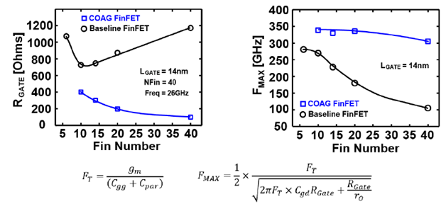
Specifically, for devices used in RF circuits, the common figure of merit (FOM) is fmax, which represents the frequency at which the biased device behavior falls to unity power gain. The greater the fmax, the greater the realizable power gain at the mmWave frequencies corresponding to 5G cellular communications.
A small-signal circuit model for the device is shown in the figure below, with an equation for fmax. Note that fmax is closely related to another FOM, ft, which represents the unity current gain frequency; a small-signal model and a relation for ft are also shown in the figure.
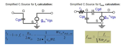
Additional items of note in the figure above include:
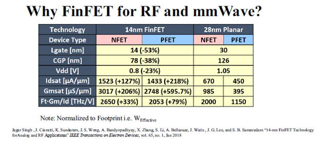
- Increasing the small-signal device transconductance, gm, increases ft and fmax. The transition from planar RF CMOS (e.g., 28nm) to FinFET technologies offers improved device gain. The figure below highlights the motivation to adopting advanced FinFET technology for RF applications. (Gmsat represents the transconductance gain for the device biased in the saturation region of operation.)
- The lower the parasitic Rgate, the higher the fmax. Reducing Rgate is the key focus of introducing the COAG process.
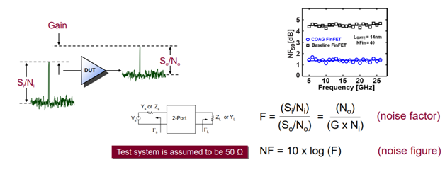
- Another critical FOM for RF CMOS technology is the “noise figure”. Each RF device in an amplifier or receiver chain introduces noise to the baseline input signal. In addition to the noise sources in the device channel (e.g., thermal, flicker), the Rgate parasitic element is also a thermal noise source. A minimal noise factor (measured in dB) is ideal – more on COAG device noise analysis shortly.
COAG analysis and reliability for 5G
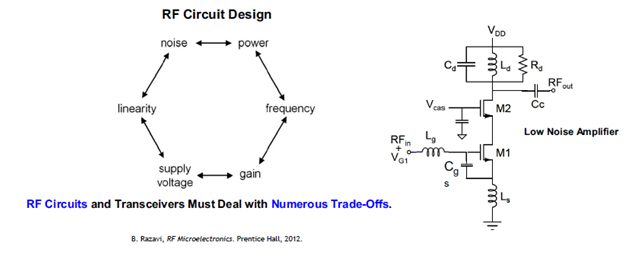
The figure below depicts the interrelated design considerations for RF CMOS, as represented by a LNA circuit topology.
At VLSI 2020, a team from GLOBALFOUNDRIES presented a thorough silicon-based analysis of the benefits of COAG on FinFET device performance for RF applications. [1]
The data for Rgate versus the number of fins is given below, for the traditional and COAG layout style. For many parallel fin devices, multiple COAG contacts are used. The substantial improvement in the fmax FOM for the COAG device is also shown below – note how the fmax for the traditional FinFET layout gate contact degrades rapidly with larger devices (# of fins).
(Note that BSIM models for FinFETs utilize a consolidated parasitic model for Rgate for many fin devices – I would encourage you to review the Rgate with NFIN model assumptions at the UC-Berkeley BSIM web site.)
The improvement in the NF50 for a 40-fin COAG device is shown below (a common source amplifier topology) – a 3dB noise reduction has a huge impact on RF circuit design. The GLOBALFOUNDRIES team also presented data isolating the Rgate noise, demonstrating that it may indeed be a significant contributor to the overall NF50 – the COAG configuration is a key factor in improving the noise factor.
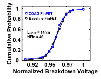
A concern with the process introduction of COAG would be the potential reliability impact of the contact and metal deposition/patterning steps directly over the gate and device oxide layers. The GLOBALFOUNDRIES team also presented TDDB reliability data for the COAG technology. Using a gate leakage current threshold measurement as the breakdown criterion, the dielectric lifetime was unaffected by the COAG process, as illustrated in the cumulative probability graph below.
The availability of COAG fabrication will undoubtedly introduce new opportunities for RF CMOS design optimizations using very wide (high fin count) devices. For more information on the GLOBALFOUNDRIES 12nm FinFET process, please follow this link.
-chipguy
References
[1] Razavieh, A., et al, “FinFET with Contact over Active-Gate for 5G Ultra-Wideband Applications”, VLSI 2020 Symposium, paper JFS2.5.
Also Read:
Embedded MRAM for High-Performance Applications
Webinar on eNVM Choices at 28nm and below by Globalfoundries
GLOBALFOUNDRIES Sets a New Bar for Advanced Non-Volatile Memory Technology
Share this post via:


Silicon Insurance: Why eFPGA is Cheaper Than a Respin — and Why It Matters in the Intel 18A Era