

The overwhelming majority of transistors produced in the world are used in memory cells, either as the memory itself (Flash, SRAM), or as the access device (DRAM). Yet, it is not necessary to have a transistor in every memory cell. In 2015, 3D XPoint, the first major product based on transistor-less memory cells, was announced [1]. Crossbar also disclosed details of their own transistor-less memory cell in the same year [2].
What makes transistor replacement attractive?
The driving force behind these developments is the reduction of memory cell footprint. The memory element can be stacked directly on top of a “selector” that acts to pass or block current, depending on the applied voltage across the cell [3]. The selector itself is smaller than a transistor as it is simply a layer stacked between electrodes. The lack of a transistor also removes the restriction to build the memory array directly on top of the silicon substrate, enabling the stacking of multiple layers to form a 3D memory array. Moreover, the circuitry that normally surrounds the memory array can now be placed underneath the array, further saving chip area.
Brief description of threshold switching
Threshold switches have actually been around for a while, in many forms, but gained particular notice after Stanford Ovshinsky published his observations of the switching behavior in disordered semiconductors in 1968 [4]. In particular, phase change memory includes the use of amorphous chalcogenides, which exhibit the following interesting behavior [3,4]:
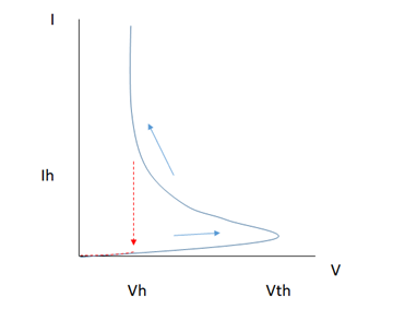
(1) The amorphous chalcogenide maintains a very high resistance up until a high enough voltage, the threshold voltage (Vth) is reached;
(2) Upon reaching the threshold voltage, the material enters an extremely conductive (“ON”) state, and the voltage across the material is reduced;
(3) The material remains in the conductive state until the voltage across it is reduced below a holding voltage (Vh), which is the voltage needed to sustain a minimum holding current (Ih). At this point, it returns to the initial high-resistance (“OFF”) state.
The behavior can be visualized in an I-V curve below:

Figure 1. I-V curve for a threshold switch. Blue: OFF-to-ON. Red: ON-to-OFF.
A wide variety of materials have been found to support threshold switching [5,6]; furthermore, a number of mechanisms have been found to be consistent with this switching:
- Metal-insulator transition [7]
- Electrothermal effect [8]
- Movement of chemical (ionic) species [5]
- Disappearance of small polarons [9]
- Order-disorder transition [6]
Regardless of the mechanism(s) involved, the special characteristics of threshold switches, particularly the occurrence of the “snapback”, i.e., the abrupt reduction of voltage after reaching Vth, lead to some important implications for the use of threshold switches.
Threshold switches can only be used with specific resistance-based memories
Threshold switches involve switching between currents orders of magnitude apart. As a result, any memory element connected in series with the threshold switch must also be able to conduct fairly high currents. This precludes the usual charge storage memories like DRAM or Flash which use insulators. Phase change memory is a more common companion to threshold switches [6]. Moreover, some of the other emerging memories may not be compatible either if they will be damaged by the sudden current surge.
Threshold switches need current compliance
Since the current surge in the ON state can be quite dramatic, a current-limiting element in series with the threshold switch is necessary to keep the current within spec. This can be a fixed resistance or an active device like a diode or a transistor. The details of this operation are quite subtle. The voltage on the cell is initially all on the threshold switch in the OFF state. Once it goes on, the voltage on the switch is reduced, so the balance of the voltage must fall on the current-limiting element. The I-V of the current-limiting element determines how much current is passed.

Figure 2. A threshold-switched cell needs a current-limiting element like a resistor to limit the current from reaching damaging levels.
Read current must exceed holding current
In order to stay ON, the threshold switch must continue to pass current larger than the holding current Ih. When the resistive memory element is being read, the threshold switch needs to be ON, so there will be a minimum read current.
The minimum read current also sets a limit on how many times the cell may be read before the memory element is disturbed, i.e., accidentally changed from one resistance state to another. This will be covered again later.
Initiation of threshold switches
Some threshold switches require an initiation (“forming”) step. Equivalently, the threshold voltage drops from its initial value, to which it can eventually recover [10]. The main concern here is whether it drops far enough that the half-selected cell voltage [3] can in fact turn ON the threshold switch.
Voltage margin can be tight
Since threshold-switched memory cells will be arranged in a crosspoint array, operation voltages will be designed accordingly. Figure 3 shows the most commonly used half-select scheme, where unselected cells in the same row or column as the selected cell necessarily receive half the voltage that the selected cell receives.

Figure 3. Crosspoint array bias schemes, enabled by the use of threshold-switched memory cells. Left: half-select scheme. Right: third-select scheme. The circle indicates the selected cell.
In this case, the maximum cell operation voltage is twice the threshold voltage Vth. For a third-select scheme, the unselected cells all receive +/- 1/3 the voltage on the selected cell. Therefore, the maximum operating voltage is 3x the threshold voltage Vth. Note that the read and write cell voltages must fall into the allowed ranges: (Vth, 2Vth) for half-select, (Vth, 3Vth) for third-select. Since the read voltage in the half-select scheme will be over half that of the write voltage, the chance of read disturb is extremely high. Even for the third-select scheme, the read voltage being over 1/3 the write voltage still poses significant risk in large arrays, as the read voltage will practically be close to 40% of the write voltage. To mitigate this, the read pulse should be very short, definitely much shorter than the write pulse.
Bottom line: cost of memories based on threshold-switching
In the end, widespread acceptance of a given memory technology depends on how effectively its cost can be driven down. Threshold switches offer a significant starting point due to their smaller footprint compared to transistors. Moreover, they are free from the usual transistor scaling issues such as short-channel effects and contact resistance dependence on doping [11, 12]. An even bigger plus is the large current density (>10 MA/cm2) that is generally available [3].
The cell size for a 1X nm DRAM is 0.0026 um2 [13], while the cell size for a 3D XPoint memory is 0.00176 um2 [14], indicating the cell size advantage already exists for a threshold-switched cell. A future cell size of 0.02 um x 0.02 um has an equivalent cell density to 100 stacked layers of 0.2 um x 0.2 um 3D NAND Flash cells, the current state-of-the-art for cell density. A larger cell size of 0.04 um x 0.04 um needs 4 stacked layers to achieve the same density. Thus, scaling threshold switches to 10 nm would provide a big boost to their becoming mainstream. That said, it also requires the readiness of the resistance-based memory element attached to the threshold switch, as mentioned above. Therefore, the replacement of transistors in memory cells by threshold switches requires the widespread acceptance of resistance-based memory as an alternative to charge-based memory.
References
[1] https://en.wikipedia.org/wiki/3D_XPoint
[2] https://ieeexplore.ieee.org/document/7104114?denied=
[3] L. Zhang, S. Cosemans, D. J. Wouters, G. Groesneken, M. Jurczak, B. Govoreanu, “One-Selector One-Resistor Cross-Point Array With Threshold Switching Selector,” IEEE Trans. Elec. Dev. 62, 3250 (2015).
[4] S. R. Ovshinsky, “Reversible Electrical Switching Phenomena in Disordered Structures,” Phys. Rev. Lett. 21, 1450 (1968).
[5] Z. Wang, M. Rao, R. Midya, S. Joshi, H. Jiang, P. Lin, W. Song, S. Asapu, Y. Zhuo, C. Li, H. Wu, Q. Xia, J. J. Yang, “Threshold Switching of Ag or Cu in Dielectrics: Materials, Mechanism, and Applications,” Adv. Func. Mat. 28, 1704862 (2018).
[6] P. Noe, A. Verdy, F. d’Acapito, J-B. Dory, M. Bernard, G. Navarro, J-B. Jager, J. Gaudin, J-Y. Raty, “Toward ultimate nonvolatile resistive memories: The mechanism behind ovonic threshold switching revealed,” Sci. Adv. 6:eaay2830, 2020.
[7] A. L. Pergament, G. B. Stefanovich, A. A. Velichko, S. D. Khanin, “Electronic Switching and Metal-Insulator Transitions in Compounds of Transition Metals https://www.researchgate.net/profile/Alex_Pergament/publication/257231373_Electronic_Switching_and_Metal-Insulator_Transitions_in_Compounds_of_Transition_Metals/links/5475ad030cf245eb4370f15e/Electronic-Switching-and-Metal-Insulator-Transitions-in-Compounds-of-Transition-Metals.pdf
[8] J. M. Goodwill, A. A. Sharma, D. Li, J. A. Bain, M. Skowronski, “Electro-Thermal Model of Threshold Switching in TaOx-Based Devices,” ACS Appl. Mater. Interfaces 9, 11704-11710 (2017).
[9] D. Emin, Polarons, Cambridge University Press, 2013, 180-185.
[10] https://thememoryguy.com/nvm-selectors-a-unified-explanation-of-threshold-switching/
[11] A. Razavieh, P. Zeitzoff, D. E. Brown, G. Karve, E. J. Nowak, “Scaling Challenges of FinFET Architecture below 40nm Contacted Gate Pitch,” 75th Annual Device Research Conference, 2017.
[12] https://www.linkedin.com/pulse/contact-resistance-silent-device-scaling-barrier-frederick-chen


Consolidation and Competition: Who is Winning the $4.5 Billion Interface IP Race?