FPGA prototyping is very popular in modeling hardware for early system prove-out, early embedded software development, as a cost-effective and performance-effective platform for software-driven hardware debug and for late-stage software debug, all before silicon is available. It has significant advantages in run-time performance over other hardware simulation methods and can be considerably less expensive than emulation. But as always, every solution comes with its own challenges; one particular challenge for FPGA prototyping is visibility into hardware internals for debug.

When using prototyping for hardware debug, good debug access is obviously critical; you have to be able to place probes / triggers wherever needed and you must be able to store long traces to debug back through sequences that may run for millions of cycles. In simulation-based verification this is easy. Changing observation points and triggers is simple and re-running after making a change to the design is equally simple.
But in FPGA prototyping neither of these steps is so easy. Take first the debug capability. Standard FPGAs, typically from Xilinx or Intel/Altera provide debug support in the form of on-chip logic analyzers (LAs), but these offer limited and potentially expensive debug support. First, they use extra gates, routing and (on-board) memory, more of each being required the more you want to debug. Problems are particularly acute with memory. Storing traces over millions of clock cycles may burn up all your on-board memory, undermining your design needs.
This becomes even more complex when your design spreads across multiple FPGAs, as is common when prototyping designs of any reasonable size. Commercial prototyping systems support large designs by partitioning them across multiple FPGAs on a board, and potentially across multiple boards or even multiple enclosures. In cases like this, native device-based debuggers hit yet another problem. They are effective, as far as they go, in debug at a device level, but each device now represents just a part of your design. Moreover, multi-FPGA prototyping isn’t just about partitioning across FPGAs. Logic to pipeline signals through limited package pins and board-level logic to optimize communication between FPGAs, all artefacts of prototyping rather than features of your design, further complicate the debug picture from a whole design point of view.
There’s another problem (in case you though you could somehow work your way around the problems I have listed so far). Since probes are logic embedded in your design, if you need to change probes (which you will, given a very limited budget for debug logic when using LAs), you’ll need to re-implement the whole design on almost all debug iterations (because you’ll almost certainly need to add more probes). And that is going to take a lot of time per iteration – adding the probes to the RTL, resynthesizing, perhaps re-partitioning and re-implementing through FPGA place and route. Think days at least to add a few probes.
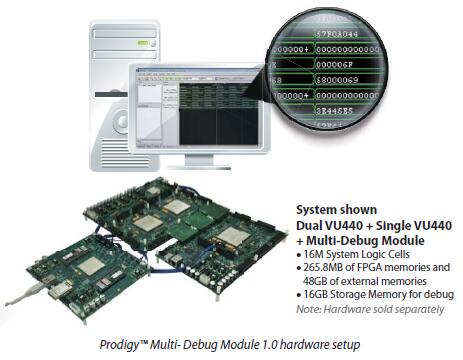
This is where dedicated debug solutions become particularly important, by moving most of the debug functionality off the FPGA so that the bulk of device resources remain allocated to your design, by supporting many more probes per device than would be possible in LAs and by letting you interact with a view of your total design (which is what you really want to understand) by transparently handling the details of design to device mapping. I’ll illustrate this through the S2C MDM (multi-debug module) solution.
On resources, consider first memory needs. MDM doesn’t use FPGA memory. All debug data is output through a DDR3 memory port to external memory on the MDM board. Freed of the highly constrained FPGA memory resources, the solution provides 16GB of memory, supporting up to 16K probes per FPGA and several million cycles of traces. The on-device support logic is also greatly reduced to the very limited circuity, even for 16K probes, needed to capture and stream out this data.
This also largely addresses the design iteration (for debug) problem. With 16K probes per FPGA, you’ll need a lot less lengthy design rebuilds to complete debug. Which means that getting to verification closure is going to be a lot faster.
Finally, the MDM solution works with up to 16 FPGAs simultaneously. And through the Prodigy Player Pro cockpit, you can interact with your design in selecting probes, viewing waveforms and tracing back to find root-causes, all without having to worry about the mapping details between the design and the FPGA implementation. Together this provide a debug solution much closer to what you are used to in simulation.
You can learn more about the S2C Multi-Debug Module HERE.
Share this post via:


Comments
There are no comments yet.
You must register or log in to view/post comments.