Events EDA2025 esig 2024 800X100

Semiconductor Ecosystem Collaboration

Semiconductor Ecosystem Collaboration
by Daniel Nenni on 02-24-2011 at 8:30 am

After 27 years in semiconductor design and manufacturing I actually had to look up the word collaboration. Seriously, I did not know the meaning of the word.

Collaboration:a recursive process where two or more people or organizations work together to realize shared goals, (this is more than the intersection of common goals seenRead More


Wally Rhines DvCon 2011 Ketnote: From Volume to Velocity

Wally Rhines DvCon 2011 Ketnote: From Volume to Velocity
by Daniel Nenni on 02-23-2011 at 1:49 pm

Abstract:
There has been a remarkable acceleration in the adoption of advanced verification methodologies, languages and new standards. This is true across all types of IC design and geographic regions. Designers and verification engineers are surprisingly open to new approaches to keep pace with the relentless rise in design… Read More


Evolution of process models, part I

Evolution of process models, part I
by Beth Martin on 02-23-2011 at 1:15 pm

441 750px dill parameters

Thirty five years ago, in 1976, the Concorde cut transatlantic flying time to 3.5 hrs, Apple was formed, NASA unveiled the first space shuttle, the VHS vs Betamax wars started, and Barry Manilow’s I Write the Songs saturated the airwaves. Each of those advances, except perhaps Barry Manilow, was the result of the first modern-era,… Read More


Custom and AMS Design

Custom and AMS Design
by Daniel Payne on 02-21-2011 at 10:06 pm

Samsung%203DIC%20Roadmap

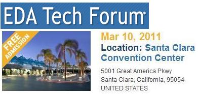
For IC designers creating full-custom or AMS designs there are plenty of challenges to getting designs done right on the first spin of silicon. Let me give you a sneak peek into what’s being discussed at the EDA Tech Forum in Santa Clara, CA on March 10th that will be of special interest to you:

3D TSV (Through Silicon Vias) are… Read More


Synopsys at Goldman Sachs Technology Conference

Synopsys at Goldman Sachs Technology Conference
by Paul McLellan on 02-21-2011 at 7:00 pm

Aart de Geus was interviewed at the Goldman Sachs Technology Conference last week. Here is some of what he said. Strong Q1, good Q2 outlook, on-track for 2011 guidance. Strong rebound in Far East, Europe mixed, North America good. 80% revenue for year booked by start of year, 90% revenue for a quarter already booked at start of quarter.… Read More


Clock Domain Crossing (CDC) Verification

Clock Domain Crossing (CDC) Verification
by Paul McLellan on 02-21-2011 at 6:12 pm

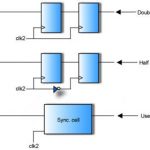
Multiple, independent clocks are quintessential in SoCs and other complex ASICs today. In some cases, such as in large communications processors, clock domains may number in the hundreds. Clock domain crossings pose a growing challenge to chip designers, and constitute a major source of design errors–errors that canRead More


Mentor Graphics Should Be Acquired or Sold: Carl Icahn COUNTERPOINT

Mentor Graphics Should Be Acquired or Sold: Carl Icahn COUNTERPOINT
by Daniel Nenni on 02-20-2011 at 7:04 pm


Daniel,

On Jan 20th, you criticized that the EDA models are all broken and need to change. Ridiculing Synpsys, Cadence, Mentor and Magma for not agreeing to ‘pay for success’ type of model (some form of royalties).

On Feb 14th, you state thatIcahn doesn’t understand EDA and should stay out. Maybe he is seeing … Read More


Mentor Graphics to Participate in SemiWiki.com Social Media Platform

Mentor Graphics to Participate in SemiWiki.com Social Media Platform
by admin on 02-17-2011 at 8:16 am


San Jose, Calif., [DATE], 2011 – SemiWiki.com today announced that Mentor Graphics, a world leader in electronic hardware and software design solutions, will participate in the SemiWiki.com global social media platform aimed at facilitating mass communication for electronic design professionals through Web 2.0 technologies.… Read More


Source of IP: Silicon foundries provides 18% of Design IP blocks, IP vendors only 16% to Fabless

Source of IP: Silicon foundries provides 18% of Design IP blocks, IP vendors only 16% to Fabless
by Eric Esteve on 02-16-2011 at 12:50 pm

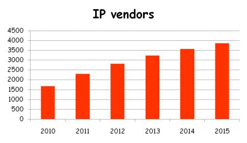
Thanks to the Semiconductor Ecosystem Survey from GSA-Wharton and the key indicators of semiconductor companies’ technology strategies related to IP:

  • IP Reuse: On average, a fabless semiconductor company reuses about 63% of design IP in the revision of an existing product design and about 44% in a new product design.
  • Source
Read More

Semiconductor Social Networking Survey Results

Semiconductor Social Networking Survey Results
by Daniel Nenni on 02-15-2011 at 9:30 pm

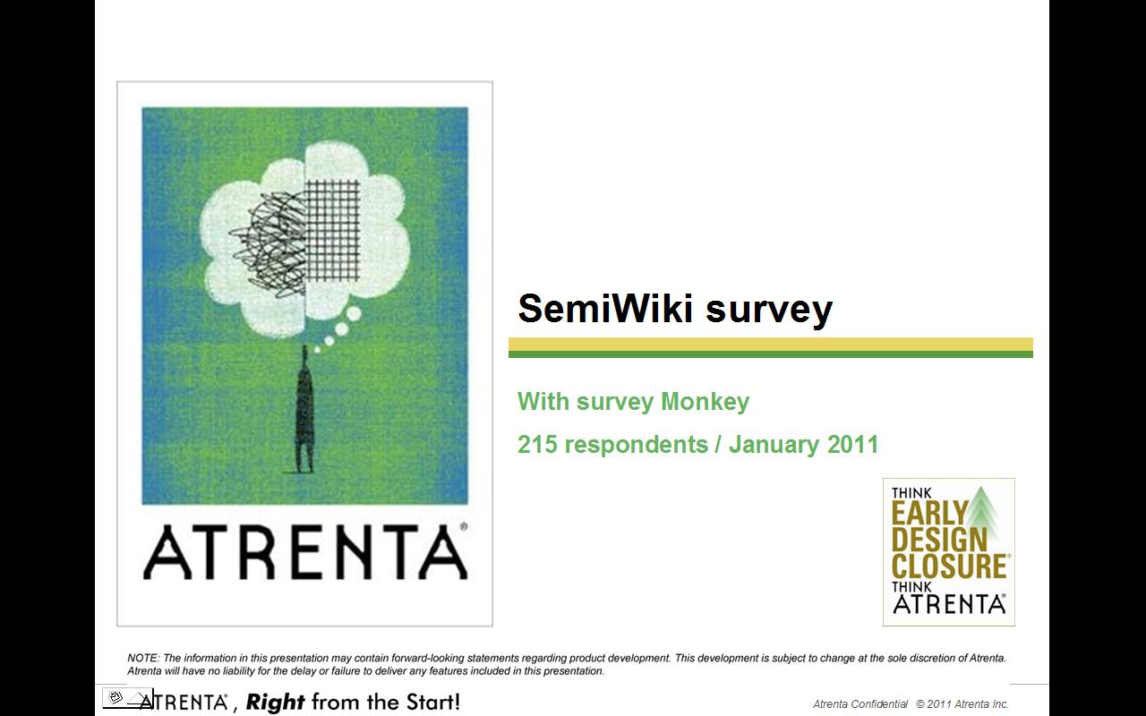
The credit here goes to Atrenta for surveying their customer base in an effort to open up new communication channels for in-demand content using Web 2.0 technologies. The results are not surprising to me but they may be to other semiconductor ecosystem executives who do not get Social Media at all!

I have been using LinkedIn for five+… Read More