On October 1, Adesto Technologies announced that it had acquired Atmel’s DataFlash and Serial Flash business groups. At first sight, this seemed a rather counter intuitive move for one of the most aggressive (and visible) companies in the emerging memory field. The purchase raised many questions to those, not least the moderator… Read More
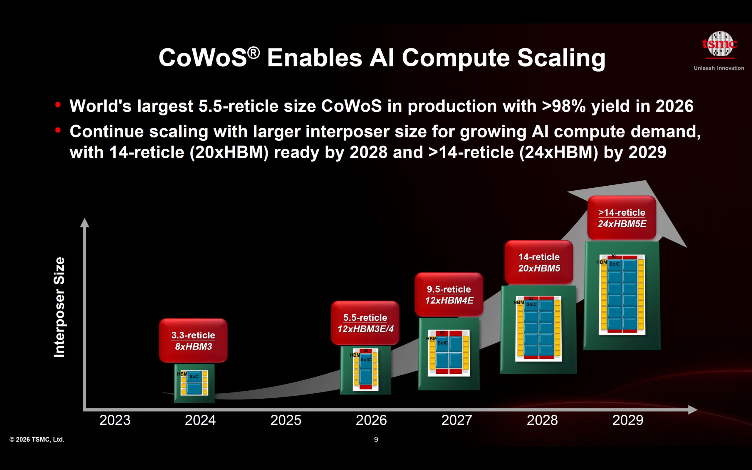 Enabling Next-Generation AI Through Advanced Packaging and 3D Fabric IntegrationThe rapid rise of artificial intelligence is fundamentally…Read More
The logic of trusting FPGAs through DO-254
Any doubters of the importance of FPGA technology to the defense/aerospace industry should consider this: each Airbus A380 has over 1000 Microsemi FPGAs on board. That is a staggering figure, especially considering the FAA doesn’t trust FPGAs, or the code that goes into them.… Read More
Jasper User Group Keynotes
I attended the Jasper User Group this week, at least the keynotes, the first by Kathryn Kranen the CEO of Jasper and the second by Bob Bentley of Intel.
Kathryn went over some history, going back to when the company was started (under the name Tempus Fugit) back in August 2002 with a single product for protocol verification. Now, since… Read More
Analog FastSPICE AMS — Simple, Fast, nm-Accurate Mixed-Signal Verification
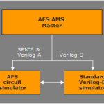
Verification and AMS are top search terms on SemiWiki so clearly designers have a pressing need for fast and accurate verification of today’s mixed-signal SoCs that include massive digital blocks and precision analog/RF circuits. They need simulation performance to verify the mixed-signal functionality, and they need nanometer… Read More
Cadence sets the Global Standards in VIP for AMBA based SoC
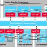
We have shown in Semiwiki how strong Cadence position was in Verification IP (VIP) in a previous post focusing on Interface standards like SuperSpeed USB or PCI Express. But IP based functions are used everywhere in a SoC, not only to interface with the external world, and need to be verified, as well, like for AMBA based functions.… Read More
Next Generation FPGA Prototyping
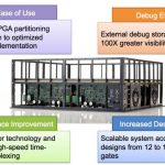
One technology that has quietly gone mainstream in semiconductor design is FPGA prototyping. That is, using an FPGA version of the design to run extensive verification. There are two approaches to doing this. The first way is simply to build an prototype board, buy some FPGAs from Xilinx or Altera and do everything yourself. The… Read More
Why are AMS designers turned off by Behavioral Modeling?
Analog Mixed-Signal (AMS) behavioral models have not caught on with the AMS designer community. Why? I suspect a significant reason (but certainly not the only one) is the way they are presented.
First, what is AMS behavioral modeling?
I define it as “a set of user-defined equations that decribe the terminal behavior of a component”.… Read More
Static Timing Analysis for Memory Characterization
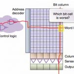
Modern SoC (System On Chip) designs contain a larger number of RAM (Random Access Memory) instances, so how do you know what the speed, timing and power are for any instance? There are a couple of approaches:
[LIST=1]
TSMC Financial Update Q4 2012!
The weather in Taiwan last week was very nice, not too hot but certainly not cold. The same could be said for the TSM stock which broke $16 after the October financial report where TSMC reported a sales increase of 15% over September. Revenues for this year thus far increased 19% over last year so why isn’t TSM stock at $20 like I predicted… Read More
Smartphone Market Share
The numbers for smartphone sales in Q3 are starting to roll in. These are in units and not yet revenue (let alone profit) numbers although everyone down to Sony is for sure profitable. Samsung is running away with the volume, selling more than Apple, Huawei and Sony put together. One name that is missing is Motorola (Google) which … Read More










Solving the EDA tool fragmentation crisis