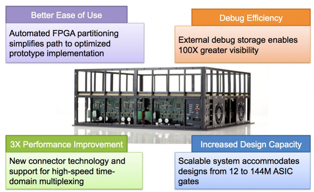
 One technology that has quietly gone mainstream in semiconductor design is FPGA prototyping. That is, using an FPGA version of the design to run extensive verification. There are two approaches to doing this. The first way is simply to build an prototype board, buy some FPGAs from Xilinx or Altera and do everything yourself. The other way is to buy a HAPS system from Synopsys, which is a more general purpose solution. Today, over 70% of ASIC designs now use some form of ASIC prototyping.
Synopsys have just announced some major upgrades to HAPS with the announcement of the HAPS-70 series and the associated software technologies.
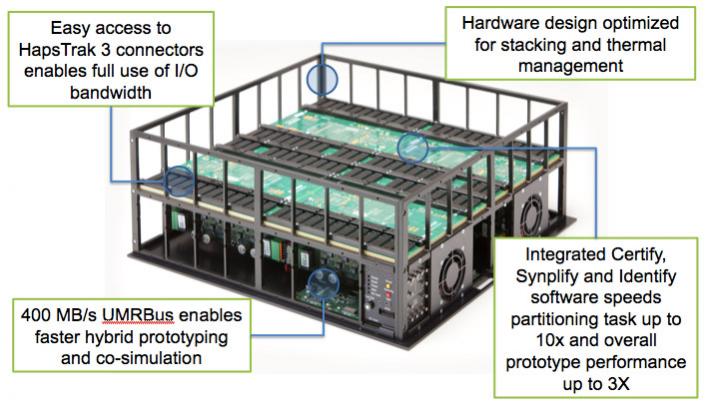
Firstly the performance of the prototype itself is increased as much as 3X by the enhanced HapsTrak I/O technology with high-speed time-domain multiplexing (HSTDM). This gives transfer rates between FPGAs in the system of up to 1 Gbps. Since all I/Os support HSTDM, this allows thousands of signals to be transferred between FPGAs and overcomes the limitation that when the design is partitioned there are often too few I/O pins for the number of signals between the partitions.
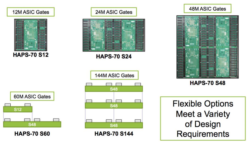 The system is modular. A single module (containing a single Xilinx FPGA) supports 12M ASIC gates. A layer in the chassis can have two or four or these, to support 24M or 48M gates respectively. And up to 3 layers extend the capacity to 144M ASIC gates. The low end is good for IP validation and the higher end for whole SoCs (and if the IP was validated using HAPS then a lot of that work automatically can be rolled over into the SoC design set up).
One of the challenges of a system like this, once the design will not fit in a single FPGA, is to partition the design into multiple FPGAs. Many systems don’t have natural partition lines, such as separating into IP blocks. There is an enhanced Certify software that automates the multi-FPGA partitioning to accelerate system bringup in HAPS. In experiments, 90% of designs could be partitioned automatically.
Another development is that it is possible to use a combination of the FPGA internal memory, external memory and the Identify software to increase the debug visibility by as much as 100 times. This is one of the big challenges of FPGA prototyping: you don’t necessarily know in advance which signals are going to turn out to be the important ones to monitor and there are too many to monitor them all, but the more data you can collect easily, the more likely that you have captured what you need when an anomaly is seen.


Comments
0 Replies to “Next Generation FPGA Prototyping”
You must register or log in to view/post comments.