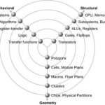
Being an internationally recognized industry blogger (IRIB) does have its benefits, one of which is free invites to all of the cool industry conferences! The presentations are canned for the most part but you can learn a lot at the breaks and exhibits if you know the right questions to ask, which I certainly do.
The GSA Semiconductor… Read More
Mask and Optical Models–Evolution of Lithography Process Models, Part IV
Will Rogers said that an economist’s guess is liable to be as good as anyone’s, but with advanced-node optical lithography, I might have to disagree. Unlike the fickle economy, the distorting effects of the mask and lithographic system are ruled by physics, and so can be modeled.
In this installment, I’ll talk about two critical… Read More
Solido & TSMC Variation Webinar for Optimal Yield in Memory, Analog, Custom Digital Design
Solido has announced webinars for North America, Europe and Asia on October 12-13. They will be describing the variation analysis and design solutions in the TSMC AMS Reference Flow 2.0 announced at the Design Automation Conference this year.
“We are pleased to broaden our collaboration with Solido in developing advanced variation… Read More
How ST-Ericsson Improved DFM Closure using SmartFill
DFM closure is a growing issue these days even at the 45nm node, and IC designers at ST-Ericsson have learned that transitioning from dummy fill to SmartFill has saved them time and improved their DFM score.
The SOC
ST-Ericsson designed an SOC for mobile platforms called the U8500 and their foundry choice was a 45nm node at STMicroelectronics… Read More
Jasper User Group Meeting
Jasper’s Annual User Group Meeting is on November 9th and 10th, in Cupertino California. It will feature users from all over the world sharing the best practices in verification. If you are a user of Jasper’s products then you should definitely plan to attend. This year there is so much good material that the meeting… Read More
Testing, testing… 3D ICs
3D ICs complicate silicon testing, but solutions exist now to many of the key challenges. – by Stephen Pateras
The next phase of semiconductor designs will see the adoption of 3D IC packages, vertical stacks of multiple bare die connected directly though the silicon. Through-silicon vias (TSV) result in shorter and thinner… Read More
Circuit Simulation and Ultra low-power IC Design at Toumaz
I read about how Toumaz used the Analog Fast SPICE (AFS) tool from BDA and it sounded interesting so I setup a Skype call with Alan Wong in the UK last month to find out how they design their ultra low-power IC chips.
Interview
Q: Tell me about your IC design background.
A: I’ve been at Toumaz almost 8 years now and before that at Sony… Read More
SuperSpeed USB finally take off! Synopsys claim over 40 USB 3.0 IP sales…
SuperSpeed USB specification was released in November 2008! Even if we can see USB 3.0 powered peripherals shipping now, essentially external HDD, connected to PC equipped with Host Bus Adaptors (as PC chipset from Intel or AMD were not supporting USB 3.0), it will take up to the second quarter of 2012 before PC will be shipped with… Read More
SoC Realization: Let’s Get Physical!
If you ask design groups what the biggest challenges are to getting a chip out on time, then the top two are usually verification, and getting closure after physical design. Not just timing closure, but power and area. One of the big drivers of this is predicting and avoiding excessive routing congestion, which is something that … Read More
Amazon’s Kindle Fire Spells Trouble for nVidia, Qualcomm and Intel
With the introduction of the Kindle Fire, it is now guaranteed that Amazon has the formula down for building the new, high volume mobile platform based on sub $9 processors. In measured fashion, Amazon has moved down Moore’s Law curve from the initial 90nm Freescale processor to what is reported to be TI’s OMAP 4 in order to add the … Read More
TSMC OIP Ecosystem Forum Preview 2024