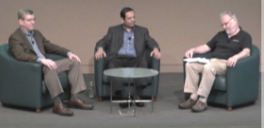
 I hosted a webinar today for GlobalFoundries. Yes, I know that today was TSMC’s Technology Symposium, we weren’t that smart when we picked the date. It was basically a “fireside chat” with me as the moderator asking the questions and Paul Colestock and Aabid Husain as my guests. We actually did it at Cadence with ChipEstimate handling the logistics. And no, there wasn’t really a fireside.
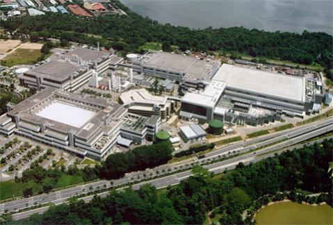
The focus was on what Global actually manufactures in Singapore. It is a mixture of stuff but increasingly they are focusing on analog, which is defined as everything that isn’t digital. We all know that the leading edge FinFET stuff gets all the publicity, and in Global’s case their big fab 8 in Saratoga, NY. But, as Paul likes to point out, leading edge for a process depends on what you are doing with it. Sure, if you want to do a state-of-the-art digital SoC is is 28-16nm depending on whether you’re in production or starting a design. But if you want to do higher voltage stuff to address the automotive market that’s not going to work. It can’t handle the voltage, it’s years away from being qualified and so on. So a leading edge analog design may be in 130nm or 90nm or 45nm. That is where analog innovation occurs. Additionally, sometimes those designs run for years and years, since the cost of redesign exceeds the potential cost saving of moving down the process node ladder.
Another aspect of analog that is good from a foundry differentiation point of view is that the process really does matter. Of course it matters in 20nm but basically those transistors are switches and secret sauce is largely in the design, from the point of view of the fabless semiconductor company selling the chip. Not the same at all in analog. Innovation is still occurring in the devices themselves, because in analog they are not just switches.
Global has put in place modular process, built up from a basic process but with extra process steps depending on what is needed on the chip. Plus specialized options like BCD. This makes it possible to mix and match stuff, adding discretes and MEMS (mechanical stuff) if appropriate, handling different voltages. They have processes going up to hundreds of volts to handle the anticipated changes in both lighting (moving to LED) and motor control (going away from AC to DC with smart controllers, which is basically what hybrid cars have today).

They are putting half-a-billion dollars of investment into their Singapore fabs to expand 300mm capacity. Some analog runs in low volume or has tiny die and doesn’t benefit that much from bigger wafers, but large die and especially anything involving bumping can benefit a lot. The cost of bumping a 300mm wafer isn’t much more than the cost for 200mm, certainly not twice as much which is (roughly) the increase in the number of die. Lots of automotive and other analog markets use gold (and other) bumping a lot. The investment takes Singapore up to around a million wafer (8″ equivalent) starts per year.
I’ve been on lots of webinars before but this was my first time where we had no presentation, we just had a Q&A. Of course we planned what we were going to talk about but we couldn’t do much more or it would sound horribly scripted. In the end, everything worked out. We talked about all the things we planned. Analog is big, growing faster than semiconductor overall, but you have to make it scalable. Modular process, 200mm and 300mm wafers, GF is ramping up capacity in Singapore to 1M wpy.
The webinar was recorded and you can watch it here. I’ve not seen the replay yet…so your mileage may vary from my memories. Thanks to the over 50 of you who preferred to watch us to Morris Chang!
Share this post via:


Is Intel About to Take Flight?